
A liquid crystal display panel, manufacturing method thereof, and display device

A technology for a liquid crystal display panel and a manufacturing method, which is applied in nonlinear optics, instruments, optics, etc., and can solve problems such as short circuit of metal wires

Active Publication Date: 2018-09-11
BOE TECH GRP CO LTD +1
View PDF7 Cites 0 Cited by
  • Summary
  • Abstract
  • Description
  • Claims
  • Application Information

AI Technical Summary

Problems solved by technology

[0003] Embodiments of the present invention provide a liquid crystal display panel, its manufacturing method, and a display device, which are used to solve the problem in the prior art that the metal line cross-over structure existing in the frame area is squeezed by the transparent liner to cause the upper and lower metal short circuit problem

Method used


Image

  • A liquid crystal display panel, manufacturing method thereof, and display device
  • A liquid crystal display panel, manufacturing method thereof, and display device
  • A liquid crystal display panel, manufacturing method thereof, and display device

Examples


Embodiment Construction

[0041] In order to make the purpose, technical solution and advantages of the present invention clearer, the present invention will be further described in detail below in conjunction with the accompanying drawings. Apparently, the described embodiments are only some of the embodiments of the present invention, rather than all of them. Based on the embodiments of the present invention, all other embodiments obtained by persons of ordinary skill in the art without making creative efforts belong to the protection scope of the present invention.

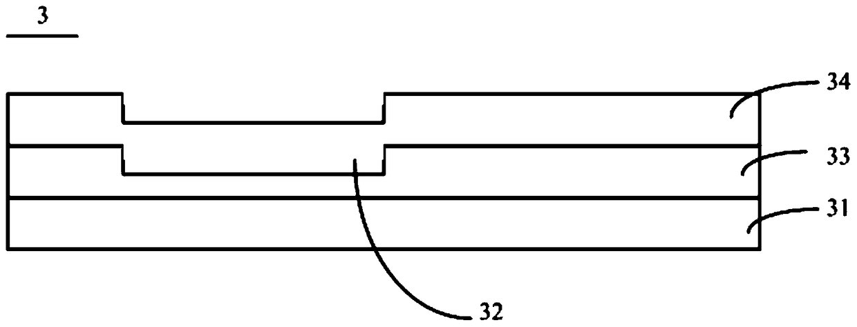
[0042] In the embodiment of the present invention, by providing at least one groove on the side of the color filter substrate close to the array substrate, the groove corresponds to a cross-over structure formed by any two insulated and overlapping metal wires in the array substrate, Moreover, the vertical projection of each groove on the array substrate can cover its corresponding cross-bridge structure, and the depth of each groove in ...


PUM

PropertyMeasurementUnit
depthaaaaaaaaaa
depthaaaaaaaaaa

Abstract

The invention discloses a liquid crystal display panel and a manufacture method and a display device thereof. The manufacture method of the liquid crystal display panel mainly comprises the steps that through the arrangement of at least one groove in the side, close to an array substrate, of a color film substrate, each groove corresponds to a cross bridging structure formed by the overlapping of any two metal wires in an insulation mode in the array substrate, each cross bridging structure can be covered with the vertical projection, in the array substrate, of the corresponding groove, and the depth, in the direction perpendicular to the direction of the array substrate, of each groove is not less than the height of the corresponding cross bridging structure. Therefore, the spacing of an air gap, located on the position where cross bridging structures exist, between the array substrate and the color film at the opposite side is in accordance with the spacing of an air gap formed in the position where cross bridging structures do not exist, enough containing space of a transparent pad in the position is guaranteed, the serious extrusion on the cross bridging structures can not occur during alignment fitting, the short circuit of an upper metal wire and a lower metal wire on each cross bridging structure is avoided, and therefore the yield of the liquid crystal display panel is improved.

Description

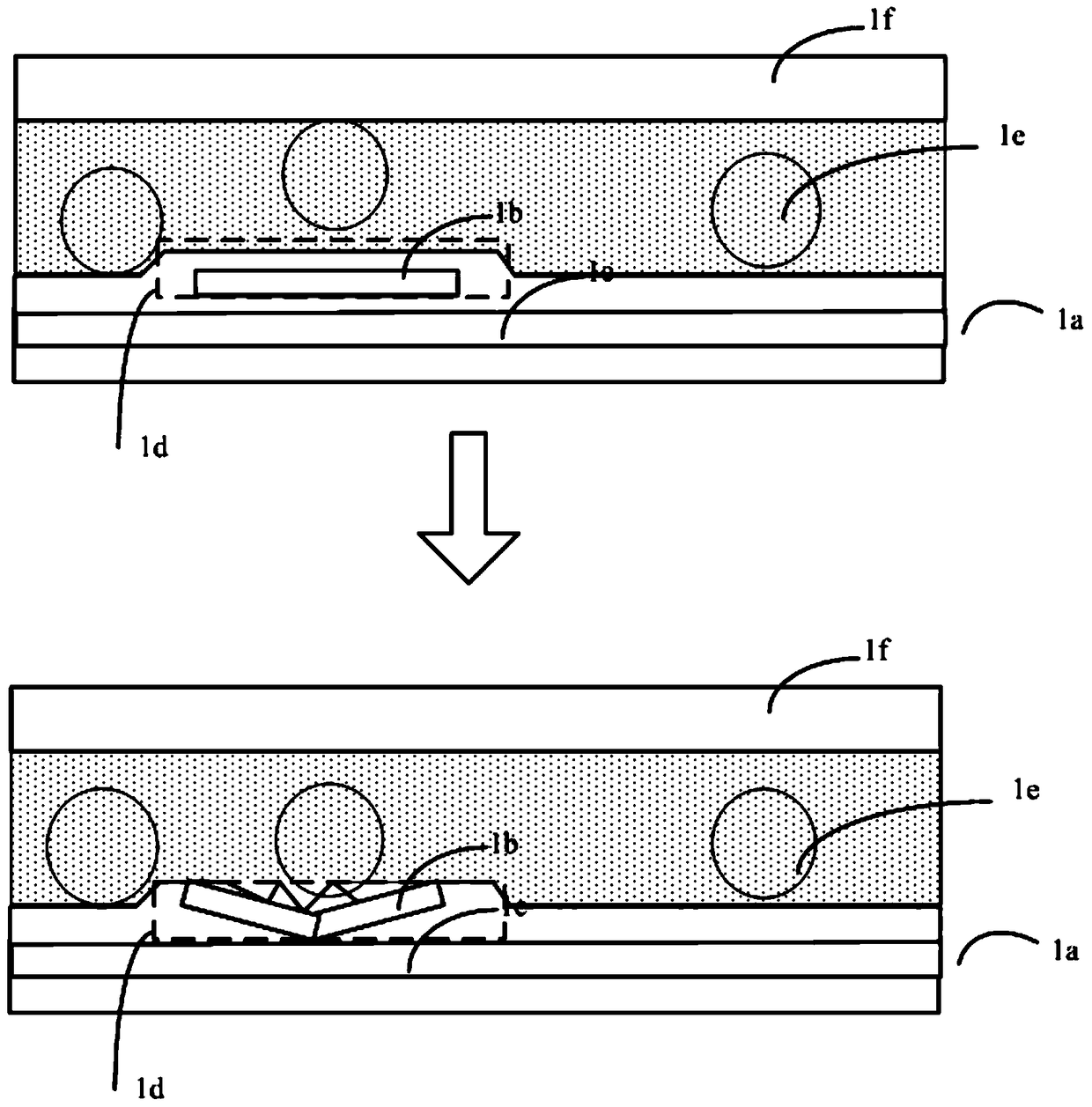
technical field [0001] The invention relates to the field of display technology, in particular to a liquid crystal display panel, a manufacturing method thereof, and a display device. Background technique [0002] In the existing liquid crystal display panel, especially for the liquid crystal display panel with a narrow frame design, in order to save the wiring space, various metal wires may be arranged in the frame area of ​​the array substrate 1a, or even two metal wires (metal wires 1b and the metal line 1c) are insulated and overlapped to form a cross bridging structure 1d. Such as figure 1 As shown, when the sealant doped with transparent liner 1e is coated on the frame area, and the upper and lower substrates are aligned and bonded, the transparent liner may just be located at the cross-over structure. The existence of the bridging structure makes the space between this position and the opposite substrate 1f smaller, and the volume of the transparent liner is small, ...

Claims


Application Information

Patent Timeline
Patent Type & Authority Patents(China)
IPC IPC(8): G02F1/1335G02F1/1333
CPCG02F1/133512G02F1/133516G02F1/1339G02F1/133302G02F1/133354
Inventor 陈华斌
Owner BOE TECH GRP CO LTD
Learn More