Method for etching silicon on the back of wet bench

An acid tank, backside technology, applied in the manufacture of electrical components, circuits, semiconductor/solid-state devices, etc., can solve the problems of abnormal appearance, difficult to take away silicon wafers in time, etc., to reduce chromatic aberration, improve economic efficiency, and improve process The effect of the process

Active Publication Date: 2015-07-08
FOUNDER MICROELECTRONICS INT
View PDF5 Cites 7 Cited by
  • Summary
  • Abstract
  • Description
  • Claims
  • Application Information

AI Technical Summary

Problems solved by technology

[0004] like Figure 5 As shown, the flushing tank 07 of the simple acid tank has no nitrogen bubbling function, but only quick discharge and overflow functions. It is difficult to remove the acid on the back of the silicon wafer and the rack 08 when flushing (using deionized water 09) The acid solution, the residual acid solution corrodes the back of the silicon wafer twice during the overflow-quick discharge process, resulting in uneven appearance
In addition, in the original flushing mode, although a large amount of acid solution on the surface of the silicon wafer can be taken away during the first quick discharge, the acid concentration on the surface of the silicon wafer is still high, and the residual acid solution will be affected by gravity after the first quick discharge. The surface of the silicon wafer flows down to form water traces

Method used


Image

  • Method for etching silicon on the back of wet bench
  • Method for etching silicon on the back of wet bench
  • Method for etching silicon on the back of wet bench

Examples


Embodiment Construction

[0036] In order to make the technical problems, technical solutions and advantages to be solved by the present invention clearer, the following will describe in detail with reference to the drawings and specific embodiments.

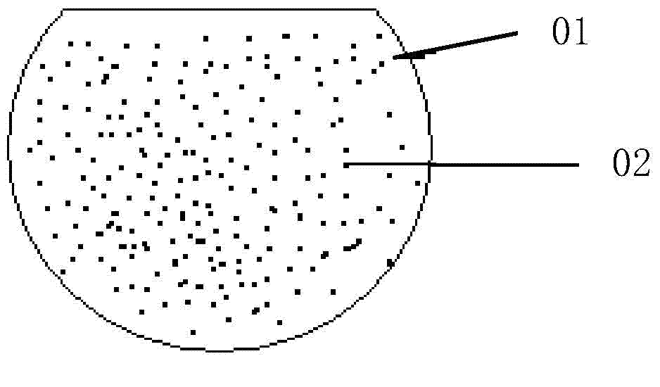
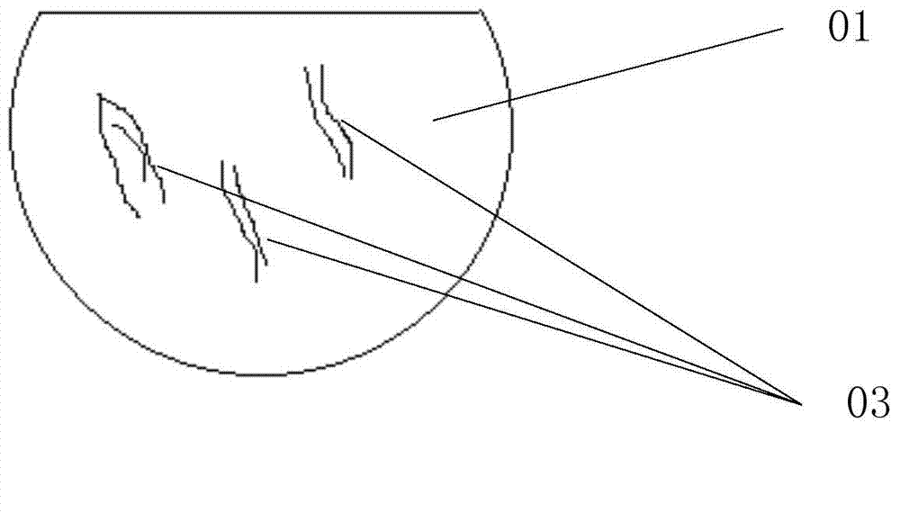
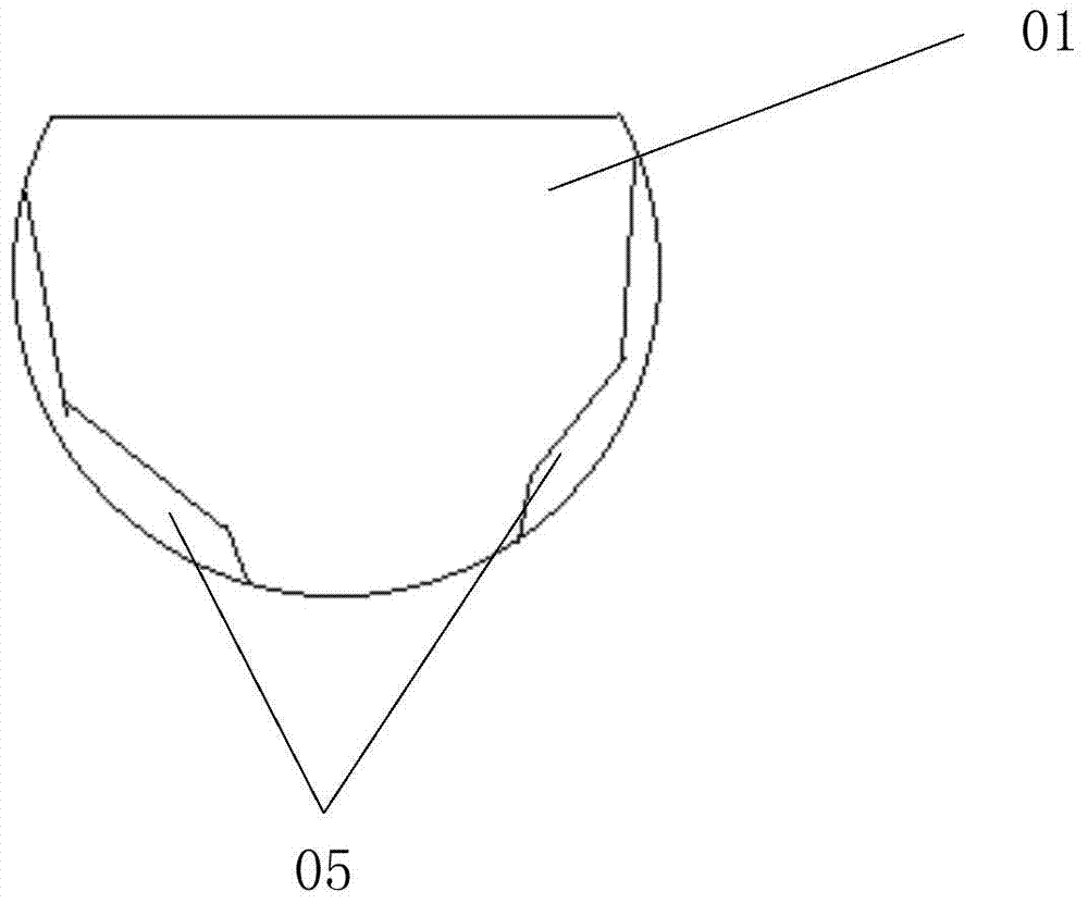
[0037] The present invention aims at the problem that apparent defects such as color difference, water marks, and film frame marks are easily formed on the back of the silicon wafer when performing silicon etching in a simple acid bath in the prior art, and provides a method for etching silicon on the back of the acid bath. Process flow, modification of the frame structure, increasing nitrogen bubbling and improving the flushing method, so that the silicon corrosion on the back of the simple acid tank meets the quality requirements, and reduces the possibility of color difference, water marks, and frame marks on the back of the silicon wafer. and improve the economic efficiency of production.

[0038] Such as Figure 9 As shown, the embodiment of the pr...


PUM


Abstract

The invention provides a method for etching silicon on the back of a wet bench, and relates to the field of semiconductor manufacturing. The method for etching silicon on the back of a wet bench comprises the steps of putting a thinned silicon wafer into deionized water into which megasonic is bubbled, putting the silicon wafer passing through the deionized water into which megasonic is bubbled into a wet bench for etching, and putting the silicon wafer after etching into a flushing tank for flushing and cleaning, thus completing silicon etching. By improving the process, reforming the wafer frame structure, increasing nitrogen bubble and improving the flushing method, etching of silicon on the back of a simple wet bench meets the quality requirements, the possibility that chromatic aberration, water stain, wafer frame mark and other appearance defects are formed on the back is reduced, and the economic benefit of production is improved.

Description

technical field [0001] The invention relates to the field of semiconductor manufacturing, in particular to a silicon etching method on the back side of an acid tank. Background technique [0002] The simple acid bath (Wet Bench) is different from the rotary etching machine (SEZ and the like), and a series of appearance abnormalities are often encountered when operating the back silicon etching process of DMOS / IGBT / Schottky products, such as water marks on the back, white stripes, Chromatic aberration etc. The silicon etching acid solution is composed of nitric acid, hydrofluoric acid, and glacial acetic acid in a certain proportion. The concentration of the solution is higher, and the silicon etching rate is faster. The simple acid tank has no stirring device, and the water tank has no bubbling, which can easily cause silicon corrosion and uneven flushing, and form apparent defects such as color difference, water marks, and film holder marks on the back of the silicon wafer...

Claims


Application Information

Patent Timeline
Patent Type & Authority Applications(China)
IPC IPC(8): H01L21/306
CPCH01L21/30604
Inventor 陈定平张忠华
Owner FOUNDER MICROELECTRONICS INT
Why Eureka
Try Eureka