Array substrate and touch-control display device and testing method thereof

A technology for array substrates and test pads, applied in the fields of array substrates and touch display devices, can solve problems such as difficulty in detecting the potential of common electrodes, short circuit between pixel electrodes and common electrodes, and influence on measurement results, so as to improve accuracy and reduce difficulty , the effect of improving accuracy

Active Publication Date: 2015-07-15
SHANGHAI AVIC OPTOELECTRONICS +1
View PDF7 Cites 36 Cited by
  • Summary
  • Abstract
  • Description
  • Claims
  • Application Information

AI Technical Summary

Problems solved by technology

Due to the limitation of the film layer structure, the common electrode multiplexed as the touch electrode is under the insulating layer, which makes it very difficult to detect the potential of the common electrode during the analysis process
Oscilloscope probes or FDP manual prober probes are not easy to pierce the insulation layer, especially when the pixel electrode is above the common electrode, it is easy to make the probe contact when piercing the probe To the pixel electrode, if violent piercing is used, it is easy to short-circuit the pixel electrode and the common electrode, which will affect the measurement results

Method used


Image

  • Array substrate and touch-control display device and testing method thereof
  • Array substrate and touch-control display device and testing method thereof
  • Array substrate and touch-control display device and testing method thereof

Examples


Embodiment Construction

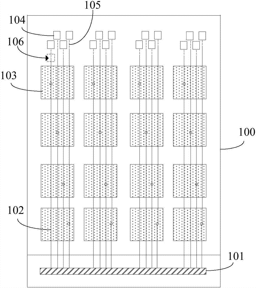
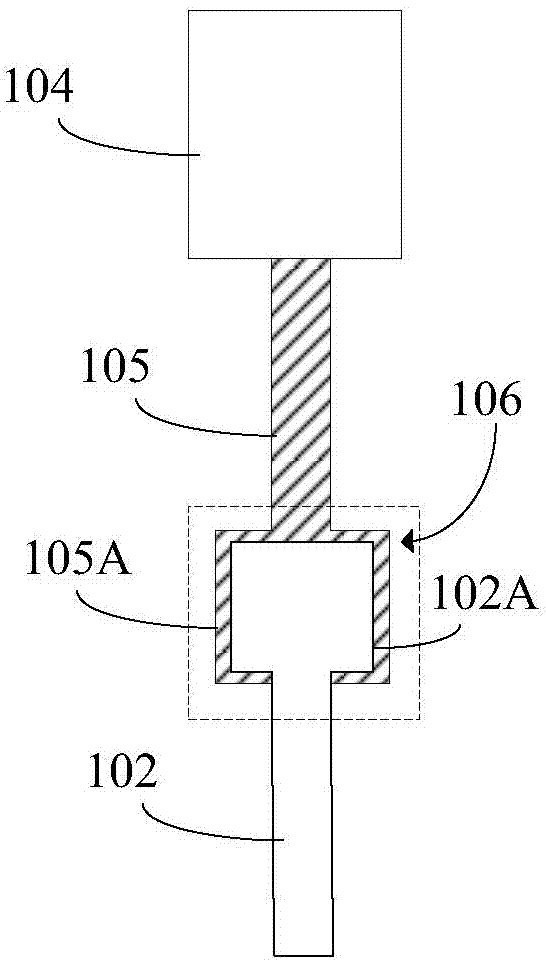
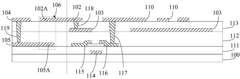
[0031] As mentioned in the background, in the prior art touch display device, the common electrodes in the pixel area are multiplexed as touch electrodes, which can reduce the size of the touch display device. Due to the limitation of the film layer structure, the common electrode multiplexed as the touch electrode is under the insulating layer, which makes it very difficult to detect the potential of the common electrode during the analysis process. Oscilloscope probes and flat panel display manual detection equipment probes are not easy to pierce the insulation layer, especially when the pixel electrode is above the common electrode, it is easy to make the probe touch the pixel electrode when piercing the probe. If you use violence If it is pierced, it is easy to short-circuit the pixel electrode and the common electrode, which will affect the measurement result.

[0032] In addition, if the common electrode is directly connected to the test terminal provided on the surface ...


PUM

PropertyMeasurementUnit
widthaaaaaaaaaa
widthaaaaaaaaaa

Abstract

The invention provides an array substrate and a touch-control display device and a testing method thereof. The array substrate comprises a substrate base, a common electrode structure and an electric conduction testing structure, wherein the common electrode structure and the electric conduction testing structure are arranged on the same side of the substrate base, and the common electrode structure and the electric conduction testing structure are mutually insulated; the projection shadows of the common electrode structure and the electric conduction testing structure in the direction perpendicular to the substrate base have an overlapped area, and the overlapped area can be subjected to laser scorification to enable the electric conduction testing structure to be electrically connected with the common electrode structure. When the electric potential of a common electrode is needed to be tested, the laser scorification can be conducted on the overlapped area, the electric conduction testing structure is electrically connected with the common electrode structure, a probe is stabbed into the electric conduction testing structure, and therefore the difficulty of common electrode potential testing is lowered, in addition, the probe is not prone to making contact with other components around the common electrode structure, and the accuracy of the testing results is improved.

Description

technical field [0001] The present invention relates to the field of display technology, in particular to an array substrate, a touch display device and a testing method thereof. Background technique [0002] As an input medium, the touch screen is currently the simplest, most convenient and natural way of human-computer interaction. Integrating a touch function on a liquid crystal display (liquid crystal display, LCD) or an organic light-emitting diode (Organic Light-Emitting Diode, OLED) display has become a research and development focus of more and more flat panel display manufacturers. [0003] In order to further reduce the volume of the touch screen and reduce the size of the mobile terminal equipped with the touch screen, in recent years, the display field has developed an in-cell touch display panel (in cell TP), which integrates touch electrodes into a liquid crystal display Therefore, the size of the touch screen using the touch display technology in the box can ...

Claims


Application Information

Patent Timeline
Patent Type & Authority Applications(China)
IPC IPC(8): G02F1/13G02F1/1343G02F1/1333G06F3/041
CPCG02F1/1309G02F1/1343G06F3/041G02F1/136254G09G3/006G09G3/3655G09G2300/0426G02F1/1345G06F3/0412G02F1/13338G06F3/04164G06F3/0443H10K59/40
Inventor 金慧俊
Owner SHANGHAI AVIC OPTOELECTRONICS
Why Eureka
Try Eureka