Method for reducing impedance mismatching degree under condition of discontinuous returning path
A technology of impedance mismatch and return path, applied in the direction of printed circuit, printed circuit, printed circuit components, etc., can solve the problems such as no high-speed signal solution, and achieve the effect of ensuring signal integrity and impedance continuity
- Summary
- Abstract
- Description
- Claims
- Application Information
AI Technical Summary
Problems solved by technology
Method used
Image
Examples
Embodiment Construction
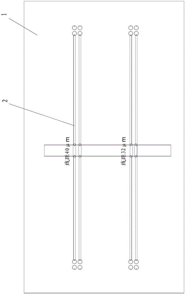
[0014] As the support and communication platform of electronic components, PCB will change its form in the arrangement of components, the fixation of the whole machine circuit and the optimization of communication signals. see figure 1 As shown, when there is a slot on the bottom reference plane under the transmission line trace of the package and the PCB, it will cause a discontinuity of impedance, which will cause the differential mode impedance of the transmission line to increase at this point. The slotted line 2 of the underlying reference plane 1 introduces an impedance discontinuity. For differential signals, this impedance mismatch will appear as a differential-mode impedance mismatch.
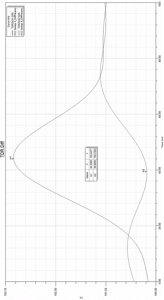
[0015] By reducing the line distance of the transmission line above the slotted line, that is, the impedance discontinuity, the differential mode impedance at this position can be reduced, so that the differential mode impedance at this position can be as close as possible to the diff...
PUM
 Abstract
Description
Claims
Application Information
 - R&D
- Intellectual Property
- Life Sciences
- Materials
- Tech Scout
- Unparalleled Data Quality
- Higher Quality Content
- 60% Fewer Hallucinations
Browse by: Latest US Patents, China's latest patents, Technical Efficacy Thesaurus, Application Domain, Technology Topic, Popular Technical Reports.
© 2025 PatSnap. All rights reserved.Legal|Privacy policy|Modern Slavery Act Transparency Statement|Sitemap|About US| Contact US: help@patsnap.com


