

Compensation method for keeping impedance continuity of wiring layer
A technology of impedance continuity and compensation method, which is applied in the direction of printed circuit making wiring diagram, computer design circuit, electrical components, etc., can solve the problem of discontinuous wiring impedance, etc., and achieve the effect of reliable design principle, simple structure and wide application prospect
- Summary
- Abstract
- Description
- Claims
- Application Information
AI Technical Summary
Problems solved by technology
Method used
Image


Examples
Embodiment Construction
[0029] In order to enable those skilled in the art to better understand the technical solutions in the present invention, the technical solutions in the embodiments of the present invention will be clearly and completely described below in conjunction with the drawings in the embodiments of the present invention. Obviously, the described The embodiments are only some of the embodiments of the present invention, not all of them. Based on the embodiments of the present invention, all other embodiments obtained by persons of ordinary skill in the art without creative efforts shall fall within the protection scope of the present invention.
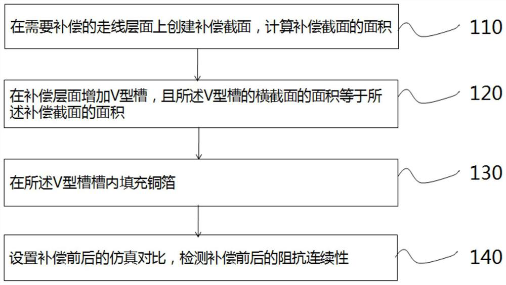
[0030] figure 1 is a schematic flowchart of a method in one embodiment of the present invention. Such as figure 1 As shown, the method includes:
[0031] Step 110, creating a compensation section on the trace level that needs to be compensated, and calculating the area of the compensation section;
[0032] Step 120, adding a V-shaped gro...
PUM
 Abstract
Description
Claims
Application Information