
A Design Method for Optimizing the Signal Quality in the Area of ​​the PCIe Connector

A technology of signal quality and design method, applied in the manufacture of printed circuits, electrical components, printed circuits, etc., can solve problems such as signal energy attenuation, bit error rate increase, inter-symbol interference, etc., to improve reflection problems and eliminate impedance steep rise , good balance

Active Publication Date: 2019-09-27
ZHENGZHOU YUNHAI INFORMATION TECH CO LTD
View PDF5 Cites 0 Cited by
  • Summary
  • Abstract
  • Description
  • Claims
  • Application Information

AI Technical Summary

Problems solved by technology

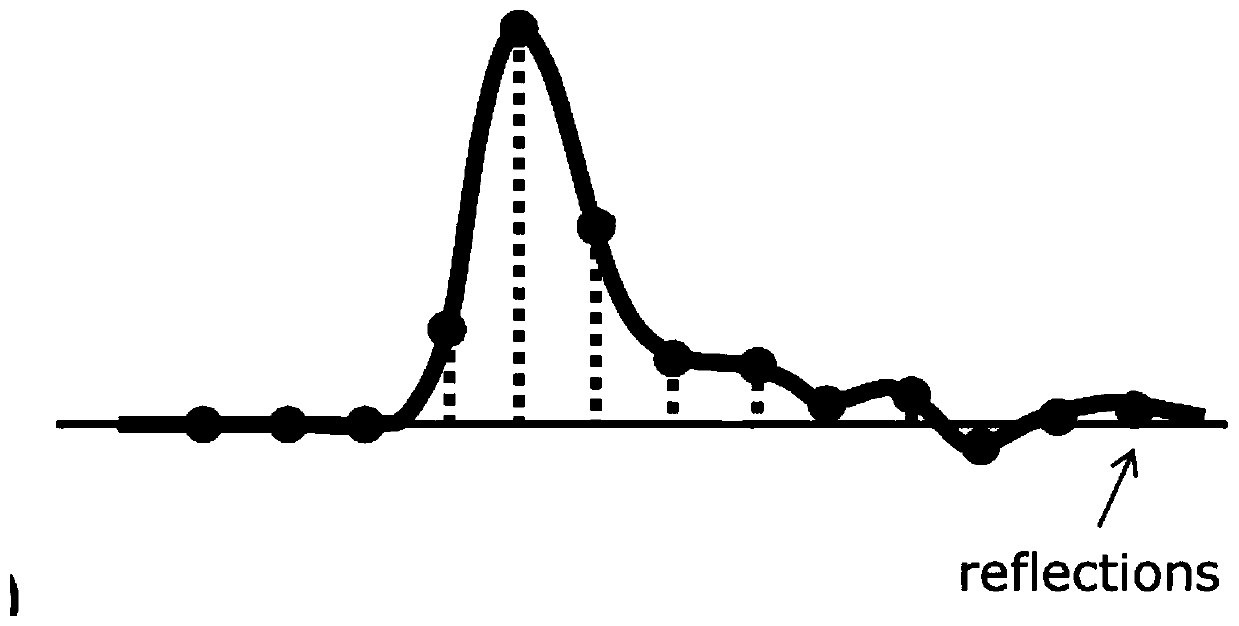
[0004] Signal reflection quantitative analysis formula: Part of the energy will be reflected back at the impedance mutation interface, and the remaining energy will continue to propagate forward. This will not only cause unnecessary consumption of energy, but more seriously, it will cause inter-symbol interference, that is to say, the reflected part of the energy will be superimposed later on the signal, such as figure 1 shown
Especially after long-distance transmission, the signal energy attenuation is serious. At this time, if there is reflection superposition, the bit error rate will increase

Method used


Image

  • A Design Method for Optimizing the Signal Quality in the Area of ​​the PCIe Connector
  • A Design Method for Optimizing the Signal Quality in the Area of ​​the PCIe Connector
  • A Design Method for Optimizing the Signal Quality in the Area of ​​the PCIe Connector

Examples


Embodiment Construction

[0028] In order to clearly illustrate the technical features of this solution, the present invention will be described in detail below through specific implementation modes and in conjunction with the accompanying drawings. The following disclosure provides many different embodiments or examples for implementing different structures of the present invention. To simplify the disclosure of the present invention, components and arrangements of specific examples are described below. Furthermore, the present invention may repeat reference numerals and / or letters in different instances. This repetition is for the purpose of simplicity and clarity and does not in itself indicate a relationship between the various embodiments and / or arrangements discussed. It should be noted that components illustrated in the figures are not necessarily drawn to scale. Descriptions of well-known components and processing techniques and processes are omitted herein to avoid unnecessarily limiting the...


PUM


Abstract

A design method for optimizing the signal quality of a PCIE connector area, comprises the following steps: S1, designing a stack layer according to the number of wiring layers required and the desired plate thickness; S2, calculating the line width and line spacing of specific signal wiring according to the stack layer and a design impedance; S3, extracting a pin model and a differential line model before reference layer compensation is performed; S4, performing reference layer compensation according to the wiring condition; S5, extracting a pin model and a differential line model after reference layer compensation is performed; and 6, performing simulation, comparing the impedances before and after reference layer compensation is performed, so as to obtain the difference, and selecting an optimal compensation quantity as a final design. The invention effectively solves the reflection problem of a signal that is caused by discontinuity of impedance, improving the signal quality, and can be widely applied to the wiring at the position of a high-speed cable connector, is an on-board wiring design method having good compatibility.

Description

technical field [0001] The invention relates to the technical field of PCB design, in particular to a design method for optimizing the signal quality of a PCIE connector area. Background technique [0002] The wiring on the PCB board has its own required characteristic impedance value (for example: single-ended signal 50ohm, PCIEGen3 signal impedance 85ohm, SATA signal impedance 100ohm, DDR4 signal impedance 40ohm, etc.). [0003] Impedance discontinuity point impedance on the transmission path is a very important parameter in signal transmission. The formula for calculating the impedance of the transmission line is: Among them, εr is the dielectric constant of the medium, H is the distance to the reference layer, W is the line width, and T is the copper thickness of the transmission line. From the impedance calculation formula, it can be known that the impedance value is proportional to H, that is to say, the distance between the transmission line and the reference plane (...

Claims


Application Information

Patent Timeline
Patent Type & Authority Patents(China)
IPC IPC(8): H05K3/00
Inventor 孙龙张长林
Owner ZHENGZHOU YUNHAI INFORMATION TECH CO LTD
Learn More