Thick metal circuit board in NFC or wireless charging technology and manufacturing method thereof

A circuit board manufacturing and wireless charging technology, which is applied in the fields of printed circuit manufacturing, chemical/electrolytic removal of conductive materials, printed circuits, etc., can solve the problems of not being able to meet the requirements of thick copper and high gap precision, and achieve strong practicability, Precise control and simple steps for the effect

Active Publication Date: 2015-08-12
SHANGHAI AMPHENOL AIRWAVE COMM ELECTRONICS CO LTD
View PDF4 Cites 9 Cited by
  • Summary
  • Abstract
  • Description
  • Claims
  • Application Information

AI Technical Summary

Problems solved by technology

However, the thickness of copper on PCB and FPC is generally only 0.07mm at present, which cannot meet the requirements of thick copper (thick conductive lines). The typical thick copper thickness requirement is 0.5mm
Since the wires are close to each ...

Method used


Image

  • Thick metal circuit board in NFC or wireless charging technology and manufacturing method thereof
  • Thick metal circuit board in NFC or wireless charging technology and manufacturing method thereof

Examples


Embodiment Construction

[0022] The present invention will be described in detail below in terms of specific embodiments in conjunction with the accompanying drawings. The following examples will help those skilled in the art to further understand the present invention, but do not limit the present invention in any form. It is to be noted that other embodiments may be utilized or structural and functional modifications may be made to the embodiments set forth herein without departing from the scope and spirit of the invention.

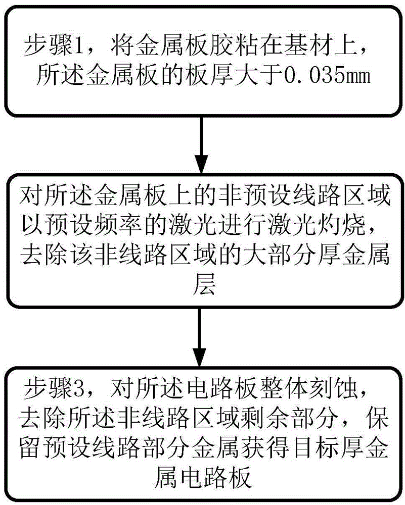
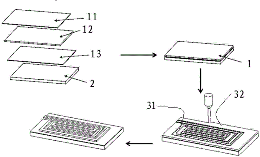
[0023] If the traditional flexible circuit board process is used to etch a thick metal circuit board, the gap cannot be made small enough, such as 0.10-0.20mm, and the etching accuracy will decrease due to the excessive thickness of the metal layer. The method provided by the invention can effectively solve the two problems of reducing the line gap and improving the etching precision. However, if the thick metal circuit board is made by winding the wire, there will be a probl...


PUM

PropertyMeasurementUnit
Plate thicknessaaaaaaaaaa

Abstract

The invention provides a manufacturing method of a thick metal circuit board in an NFC or wireless charging technology, which is characterized by comprising the steps 1, adhering a metal plate to a base material, wherein the thickness of the metal plate is greater than 0.035mm; 2, carrying out laser burning on a non-preset circuit region on the metal plate by laser with preset frequency, and removing most of a thick metal layer on the non-circuit region; and 3, carrying out etching on the whole circuit board, removing residue of the non-circuit region, and retaining a preset circuit portion so as to acquire the target thick metal circuit board. Application of the method provided by the invention can enable manufacturing of an NFC or wireless charging antenna to be not restricted in base material selection, and can also realize accurate control for an interval of adjacent wires through controlling a laser burning region. The thick metal circuit board in the NFC or wireless charging technology and the manufacturing method thereof are simple in step and high in practicability.

Description

technical field [0001] The invention relates to the technical field of antenna production, in particular to a thick metal circuit board with NFC or wireless charging technology and a production method thereof. Background technique [0002] The current manufacturing method of coils in NFC or wireless charging technology is to use PCB or FPC as the substrate of the circuit board to plate copper or wire. However, the thickness of copper on PCB and FPC is generally only 0.07mm at present, which cannot meet the requirements of thick copper (thick conductive lines). The typical thick copper thickness requirement is 0.5mm. Since the wires are close to each other, the traditional manufacturing method is difficult to meet the gap requirements between adjacent antenna wires in NFC or wireless charging technology, and the gap accuracy requirements of NFC or wireless charging technology are generally Both are very high. [0003] Therefore, how to make a circuit board that meets the re...

Claims


Application Information

Patent Timeline
IPC IPC(8): H05K3/02H05K3/06
CPCH05K3/022H05K3/027H05K3/06H05K2203/107
Inventor 钱鹏陈德智
Owner SHANGHAI AMPHENOL AIRWAVE COMM ELECTRONICS CO LTD
Why Eureka
Try Eureka