Method of fabricating solar cells with p-doped cdte layers of reduced thickness

A technology of solar cells and doped layers, applied in the direction of final product manufacturing, sustainable manufacturing/processing, circuits, etc., can solve problems such as limitations

Active Publication Date: 2019-12-31
CHINA TRIUMPH INT ENG +1
View PDF5 Cites 0 Cited by
  • Summary
  • Abstract
  • Description
  • Claims
  • Application Information

AI Technical Summary

Problems solved by technology

High p-doping of CdTe is limited by formation self-compensation, as predicted by theory

Method used


Image

  • Method of fabricating solar cells with p-doped cdte layers of reduced thickness
  • Method of fabricating solar cells with p-doped cdte layers of reduced thickness
  • Method of fabricating solar cells with p-doped cdte layers of reduced thickness

Examples


Embodiment Construction

[0042] In the following, the method according to the invention is explained in a first exemplary embodiment showing the production of a solar cell in a layer structure, without any limitation being meant for said embodiment.

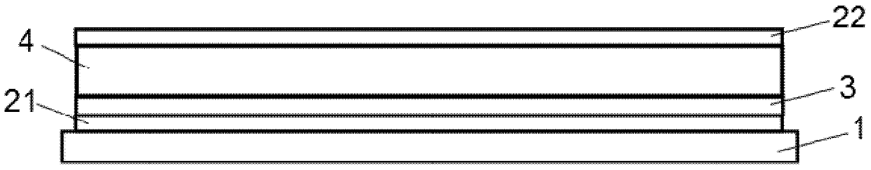
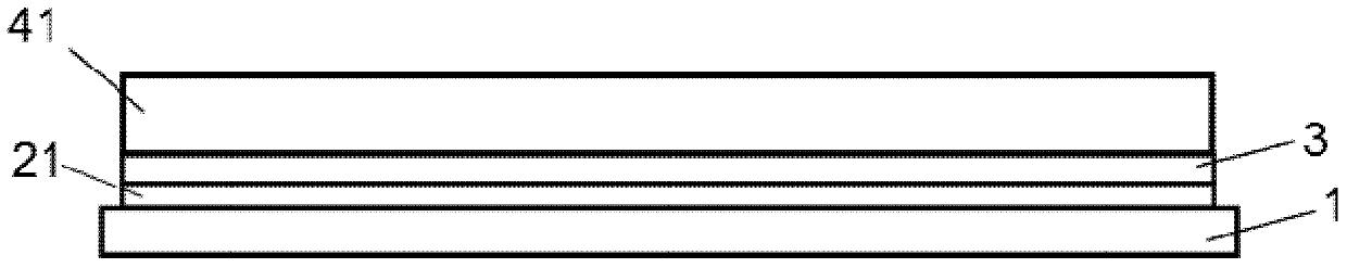
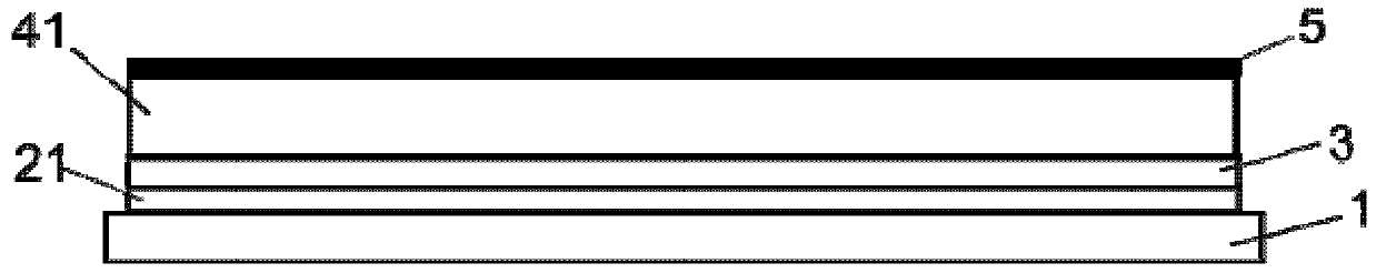
[0043] as in Figure 2a As shown in , the front contact (21) and the CdS layer (3) have been applied on the transparent substrate (1) by means of methods according to the prior art. As a front contact ( 21 ), a 450 nm thick transparent bilayer [fluorine-doped tin oxide (350 nm) as conductive layer and tin oxide (100 nm) as high-resistance buffer layer] was applied (as TCO). The CdS layer (3) reaches a thickness of 90nm and is deposited using the CSS technique. On it, a first CdTe layer ( 41 ) according to the invention is deposited with a thickness of 1.6 μm. The deposition process was carried out as a CSS process at a substrate temperature of 530°C, resulting in large grains of the deposited layer.

[0044] Figure 2b A sacrificial doped layer (5) a...


PUM


Abstract

The invention relates to a method for manufacturing a solar cell with a thin p-doped CdTe layer, and particularly, relates to a method for manufacturing a thin-film CdTe solar cell. The thin-film CdTe solar cell has a CdTe layer with a reduced layer thickness, without pin holes and being uniformly doped. The method is adopted for preventing solar cell shunting, improving the reliability and the long-term stability of the solar cell, and providing an effective method for uniform doping of the CdTe layer. The method is realized by applying a sacrificial doping layer between a first CdTe layer with a large grain and a second CdTe layer with a small grain, and the first CdTe layer and the second CdTe layer form the CdTe layer of the solar cell. In addition, the sacrificial doping layer includes halogen, so that CdC12 activation processing is not needed.

Description

technical field [0001] The object of the present invention is a method of manufacturing CdTe solar cells with increased efficiency. Background technique [0002] The distribution of thin-film solar cells can be further accelerated by increasing their electrical efficiency in terms of light conversion. CdTe-based solar cells have proven particularly promising in this regard. [0003] In the prior art, CdTe solar cells have the following structure: a transparent conductive oxide layer (TCO) is deposited as a front contact on a glass substrate. The TCO layer can include a high resistance buffer layer that helps minimize shunting effects in the solar cell. On top of that, a layer of cadmium sulfide (CdS) is deposited and on top of that a layer of cadmium telluride (CdTe). Finally, a metal layer is applied to collect charge carriers. This approach is called superstructure. [0004] During the production of solar cells, the substrate, preferably glass, forms the matrix on whi...

Claims


Application Information

Patent Timeline
Patent Type & Authority Patents(China)
IPC IPC(8): H01L31/18H01L31/0264
CPCH01L31/02963H01L31/0445H01L31/073H01L31/1836Y02E10/543Y02P70/50
Inventor 克里什纳库马·维拉潘彭寿
Owner CHINA TRIUMPH INT ENG
Why Eureka
Try Eureka