
Array substrate

An array substrate and thin film transistor technology, applied in nonlinear optics, instruments, optics, etc., can solve the problem of whitening on both sides of the display, and achieve the effect of improving the whitening on both sides and improving the large viewing angle deviation.

Active Publication Date: 2017-09-15
TCL CHINA STAR OPTOELECTRONICS TECH CO LTD
View PDF6 Cites 0 Cited by
  • Summary
  • Abstract
  • Description
  • Claims
  • Application Information

AI Technical Summary

Problems solved by technology

[0004] The purpose of the present invention is to provide an array substrate to solve the technical problem of whitening on both sides of the existing liquid crystal display

Method used


Image

  • Array substrate
  • Array substrate
  • Array substrate

Examples


Embodiment 1

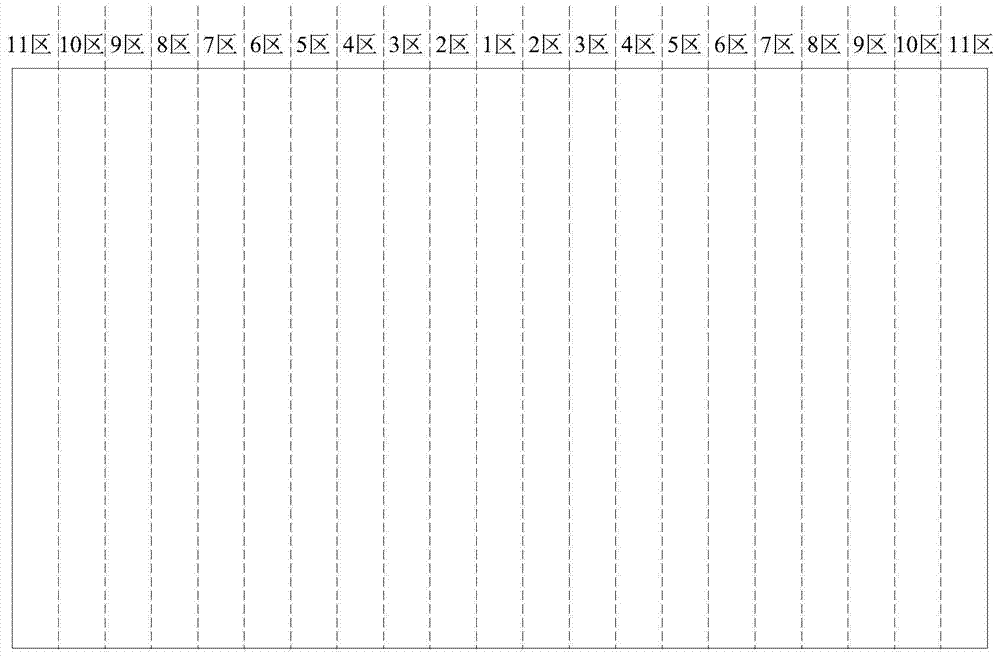
[0046] An embodiment of the present invention provides an array substrate, including a plurality of sub-pixel units, a scanning line and a common electrode line corresponding to each row of sub-pixel units, and a data line corresponding to each column of sub-pixel units. In the extending direction of the scanning lines, the array substrate is divided into multiple regions, such as image 3 As shown, this embodiment is divided into 21 areas altogether. Among them, the area in the middle can be called District 1, and there are 10 areas on both sides of District 1, which are District 2 to District 11 in turn.

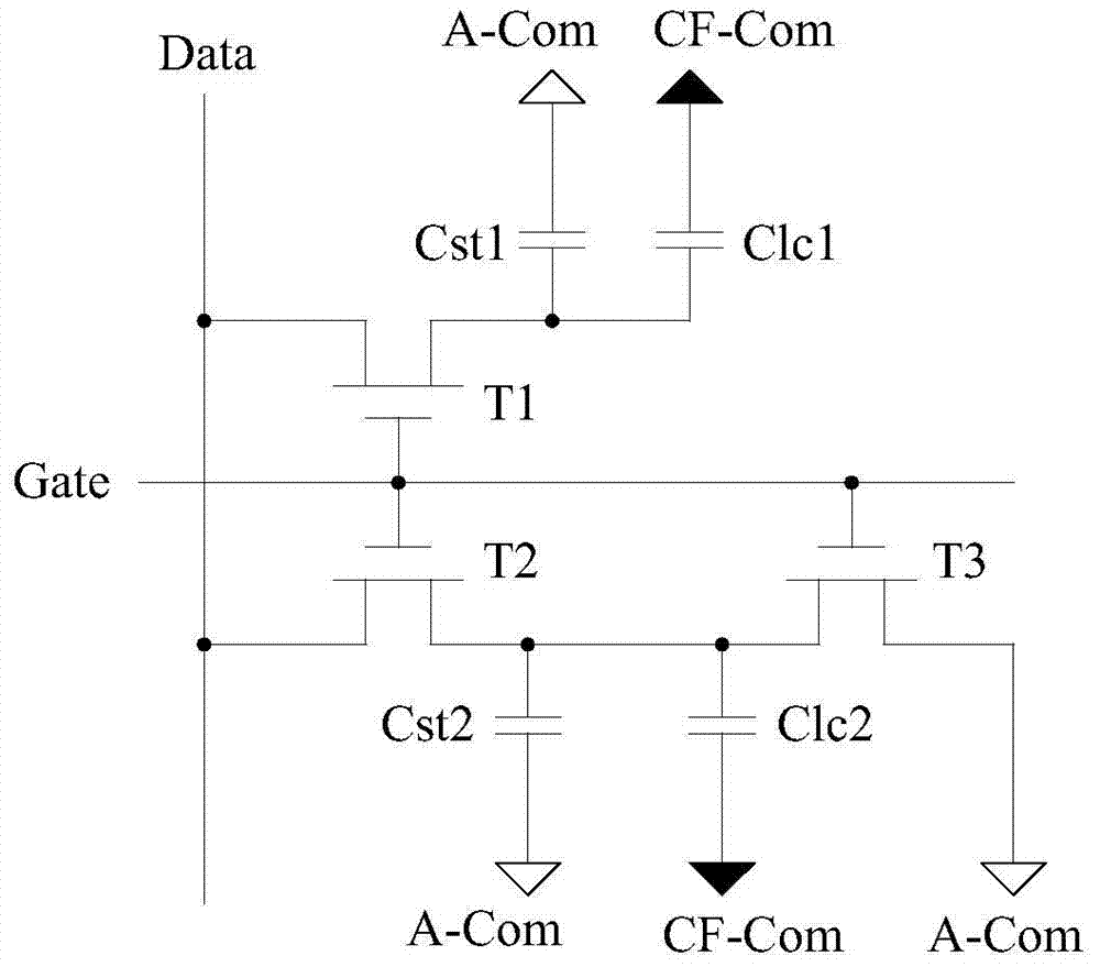
[0047] Such as Figure 4a and Figure 4b As shown, the sub-pixel unit in this embodiment adopts a low color shift design, and each sub-pixel unit includes a main pixel electrode 101, a sub-pixel electrode 102, a first thin film transistor T1, a second thin film transistor T2 and a third thin film transistor T3. Gates of T1 , T2 and T3 are connected to the same scan lin...

Embodiment 2

[0056] This embodiment is basically the same as Embodiment 1, the difference being that in this embodiment, T3 in each sub-pixel unit has a horseshoe-shaped structure. Such as Figure 6 As shown, the channel of a horseshoe-shaped thin film transistor usually includes an arc portion and a straight portion, wherein the parameters about the channel size mainly include the inner diameter a of the arc portion, the outer diameter b of the arc portion, and the length c of the straight portion. The channel width-to-length ratio of a horseshoe-shaped TFT can be expressed as:

[0057]

[0058] In this embodiment, the channel width-to-length ratio of T3 in different regions is adjusted by adjusting the size of the outer diameter b of the arc-shaped portion.

[0059] Such as Figure 7a and Figure 7b As shown, in all 21 regions of the array substrate, the inner diameter a of the arc portion of the channel of T3 is 2 micrometers, and the length of the straight portion of the channel ...


PUM


Abstract

The invention discloses an array substrate, belongs to the field of display technology, and solves the problem that two sides of an existing liquid crystal display are whitened. The array substrate comprises a plurality of sub pixel units, and each sub pixel unit comprises a primary pixel electrode, a secondary pixel electrode, a first thin film transistor, a second thin film transistor and a third thin film transistor. In the extension direction of a scanning line, the breadth length ratio of channels of the third thin film transistors in the sub pixel units positioned in the middle of the array substrate is smaller than that of the third thin film transistor in the sub pixel units positioned at two ends of the array substrate.

Description

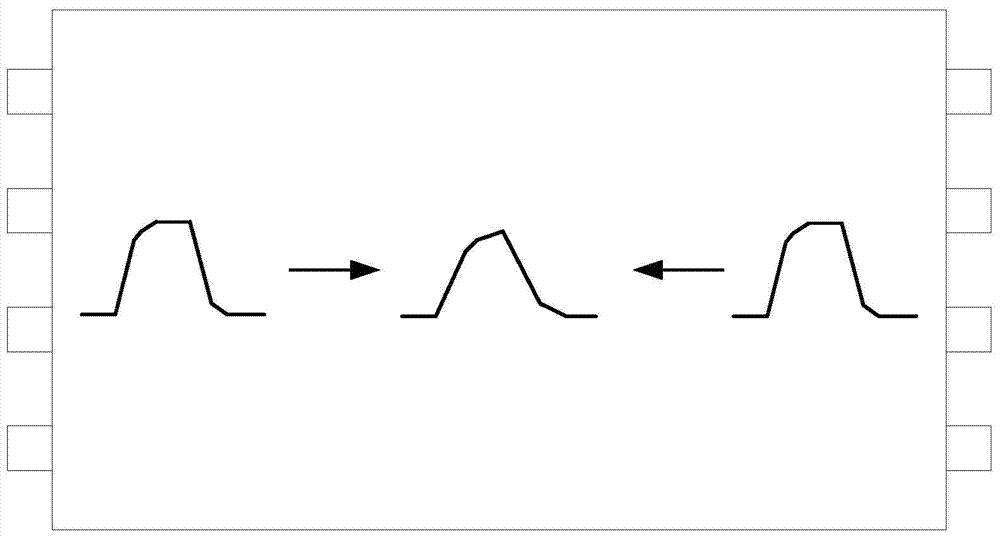
technical field [0001] The present invention relates to the field of display technology, in particular to an array substrate. Background technique [0002] With the development of display technologies, liquid crystal displays have become the most common display devices. In a liquid crystal display, the grayscale displayed by each sub-pixel unit is controlled by a plurality of interlaced scanning lines and data lines, so as to realize the display of the entire image. [0003] Such as figure 1 As shown, the scanning signal transmitted by the scanning line is input from the Chip On Film (COF) on the left and right sides of the liquid crystal. Because of the RC delay of the scanning line itself, the original normal waveform when the scanning signal is input will be transmitted to the Distortion occurs after the middle, and the distorted scanning signal will reduce the charging rate of the sub-pixel unit in the middle of the liquid crystal panel, reduce the brightness in the mi...

Claims


Application Information

Patent Timeline
Patent Type & Authority Patents(China)
IPC IPC(8): G02F1/1362G02F1/1368G02F1/133
CPCG02F1/133G02F1/136286G02F1/1368G02F1/139
Inventor 刘桓
Owner TCL CHINA STAR OPTOELECTRONICS TECH CO LTD
Learn More