
Preparation method of transmission electron microscope samples

An electron microscope and sample technology, applied in the preparation of test samples, etc., can solve the problems of imaging drift, time-wasting, easy to cause undercut, etc., achieve good thickness uniformity, avoid imaging drift, and improve preparation efficiency.

Active Publication Date: 2018-01-02
SEMICON MFG INT (SHANGHAI) CORP
View PDF3 Cites 0 Cited by
  • Summary
  • Abstract
  • Description
  • Claims
  • Application Information

AI Technical Summary

Problems solved by technology

In addition, using such a method, it is easy to cause undercut in the obtained TEM sample 100, as shown in the region 100a
[0008] As above, the TEM sample preparation method of the prior art has many disadvantages, for example, sample damage caused by undercuts is prone to occur during the FIB bombardment process, the true morphology is hidden due to the uneven thickness of the TEM sample, and the blind layer removal operation (blind Delayer) caused by over polishing (over polish), the whole process is a waste of time when preparing larger samples, and it is easy to cause imaging blur or imaging drift in the process of preparing TEM samples, etc.
And when the above problems are encountered, it is often necessary to rework

Method used

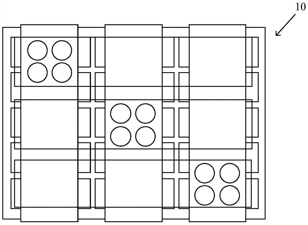
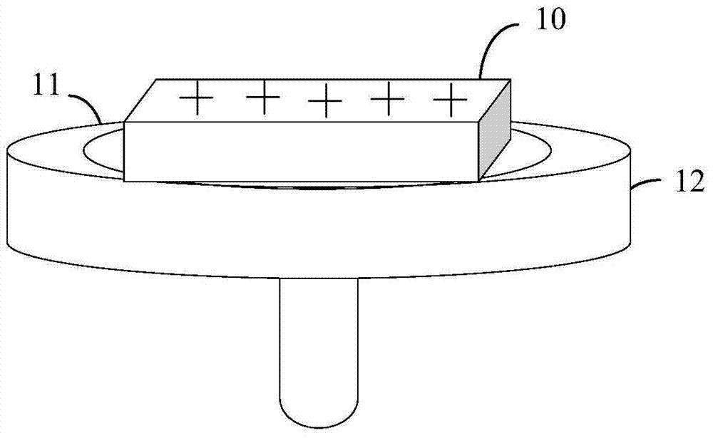
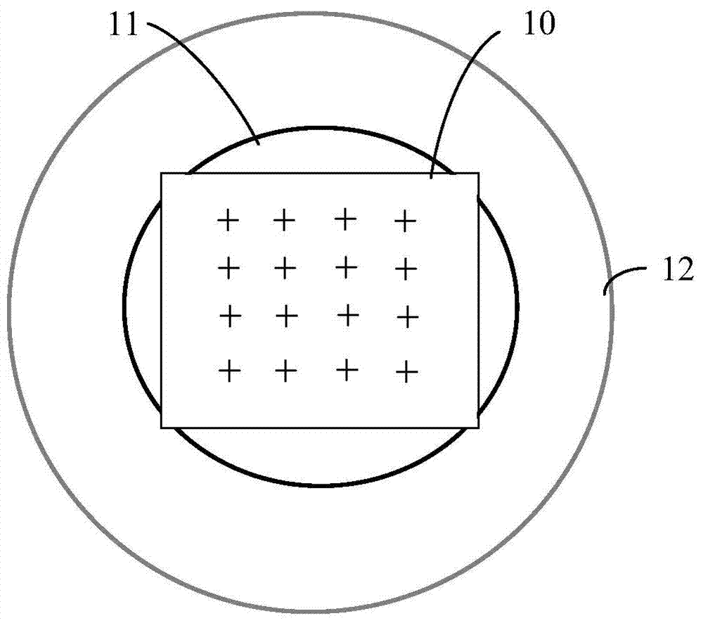

Image

  • Preparation method of transmission electron microscope samples
  • Preparation method of transmission electron microscope samples
  • Preparation method of transmission electron microscope samples

Examples


Embodiment Construction

[0048] The present invention will be further described below in conjunction with specific embodiments and accompanying drawings, but the protection scope of the present invention should not be limited thereby.

[0049] refer to Figure 7 , the TEM sample preparation method of the present embodiment comprises the following steps:

[0050] Step S21, providing a sample with length, width and thickness, the sample has an observation target, and the observation target includes at least one elongated structure or multi-layer stacked structure along the thickness direction;

[0051] Step S22, mark the surface of the sample defined by the length and width directions, and the distance between the mark and the observation target is within a preset distance range;

[0052] Step S23, grinding the sample to the mark along a direction perpendicular to the thickness direction;

[0053] Step S24, placing the sample on the carrier platform, the grinding surface of the sample is away from the c...


PUM

PropertyMeasurementUnit
depthaaaaaaaaaa

Abstract

The present invention provides a method for preparing a transmission electron microscope sample, comprising: providing a sample with length, width and thickness, and having an observation target on the sample, and the observation target includes at least one elongated structure or multilayer stack along the thickness direction structure; mark the surface of the sample defined by the length and width directions, and the distance between the mark and the observation target is within a preset distance range; grind the sample to the mark in the direction perpendicular to the thickness direction; set the sample on the carrier On the above, the grinding surface of the sample is away from the carrying platform, and the opposite surface of the grinding surface faces the carrying platform; a conductive film is formed on the back of the sample to electrically connect the sample to the carrying platform; the grinding surface is processed by using a focused ion beam, An observation sample containing the observation target is obtained. The invention can improve the preparation efficiency and the hit rate, and can avoid the problem of imaging blur or image drift caused by charge accumulation in the sample preparation process.

Description

technical field [0001] The invention relates to a semiconductor material analysis technology, in particular to a preparation method of a transmission electron microscope sample. Background technique [0002] With the development of semiconductor technology, the complexity and integration of integrated circuits continue to increase. The number of devices integrated on a single chip has reached hundreds of millions or even billions. Challenges are presented, such as optical microscopy (OM) and scanning electron microscopy (SEM) have not been able to meet the requirements. Due to the high resolution of the Transmission Electron Microscope (TEM, Transmission Electron Microscope) can observe the internal structure of the thin film region, so with the continuous improvement of the semiconductor process level, especially after entering the 130nm process, the Transmission Electron Microscope has become an important tool for observation and analysis. Necessary means for the internal...

Claims


Application Information

Patent Timeline
Patent Type & Authority Patents(China)
IPC IPC(8): G01N1/28
Inventor 殷原梓杨梅高保林张菲菲
Owner SEMICON MFG INT (SHANGHAI) CORP
Learn More