A method and device for processing output voltage ripple of a charger
A technology of output voltage ripple and output voltage, which is applied in the field of processing the output voltage ripple of chargers, and can solve problems such as large power frequency ripple
- Summary
- Abstract
- Description
- Claims
- Application Information
AI Technical Summary
Problems solved by technology
Method used
Image
Examples
Embodiment 1
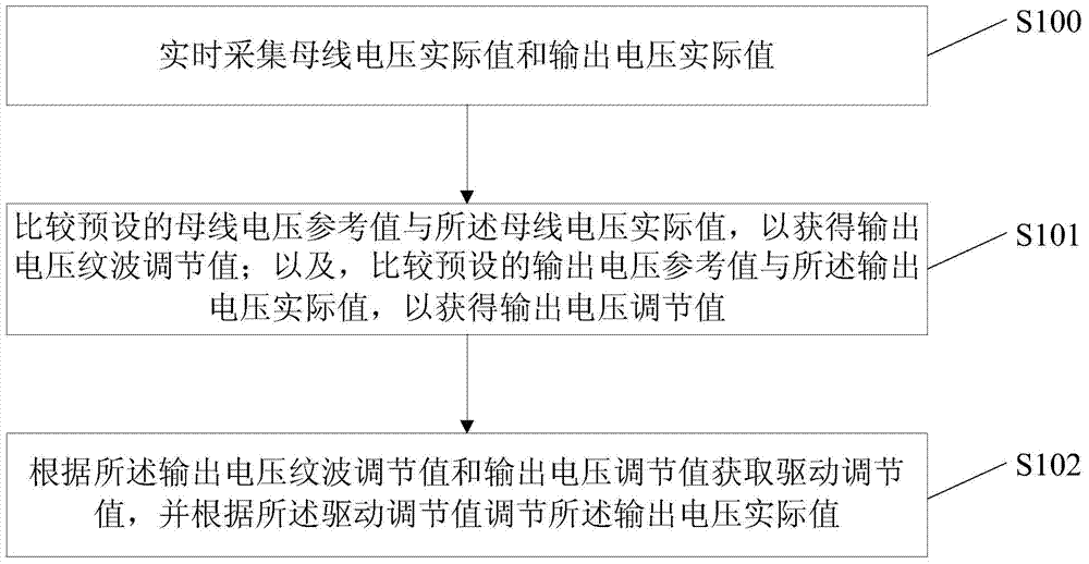
[0022] figure 1 It is a flow chart of the method for processing the output voltage ripple of the charger provided by Embodiment 1 of the present invention. The technical solution of this embodiment is applicable to the situation where the output voltage of the charger is adjusted to suppress the output voltage ripple. The method can be executed by a processing device for output voltage ripple of the charger, and the device can be implemented in the form of software and / or hardware, and is configured to be executed in a main control chip of the charger. see figure 1 As shown, the method for processing the output voltage ripple of the charger specifically includes the following steps:
[0023] Step S100, collecting the actual value of the bus voltage and the actual value of the output voltage in real time.
[0024] The voltage detection device (such as a sensor) contained in the charger itself can be used to collect the actual value of the bus voltage and the actual value of ...
Embodiment 2
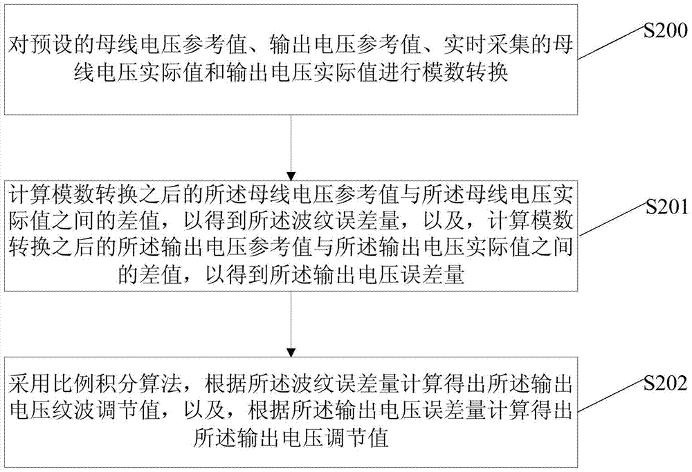
[0032] Figure 2a It is a flow chart of the method for processing the output voltage ripple of the charger provided by the second embodiment of the present invention. On the basis of the first embodiment of the present invention, the method for processing the output voltage ripple of the charger further compares a preset bus voltage reference value with the actual bus voltage value to obtain an output voltage ripple adjustment value; and, Comparing the preset output voltage reference value with the actual output voltage value to obtain the output voltage adjustment value, the specific optimization is:
[0033] Perform analog-to-digital conversion on the preset bus voltage reference value, output voltage reference value, real-time collected bus voltage actual value and output voltage actual value;
[0034] calculating the difference between the bus voltage reference value after analog-to-digital conversion and the bus voltage actual value to obtain the ripple error amount, and...
Embodiment 3
[0050] image 3 It is a schematic structural diagram of a processing device for output voltage ripple of a charger provided in Embodiment 3 of the present invention. see image 3 As shown, the processing device for the output voltage ripple of the charger includes:
[0051] The voltage acquisition module 300 is used to acquire the actual value of the bus voltage and the actual value of the output voltage in real time;
[0052] A digital signal processing module 310, configured to compare a preset reference value of the bus voltage with the actual value of the bus voltage to obtain an output voltage ripple adjustment value; and, compare a preset reference value of the output voltage with the actual value of the output voltage , to obtain the output voltage adjustment value;
[0053] The voltage adjustment module 320 is configured to obtain a driving adjustment value according to the output voltage ripple adjustment value and the output voltage adjustment value, adjust the ac...
PUM
 Abstract
Description
Claims
Application Information


