

Manufacturing method for PCB golden finger
A production method and gold finger technology, which are applied in the direction of the formation of electrical connection of printing elements, can solve problems such as the inapplicability of the gold finger production process, and achieve the effect of preventing the gold finger gap and the side bulge of the gold finger.
- Summary
- Abstract
- Description
- Claims
- Application Information
AI Technical Summary
Problems solved by technology
Method used
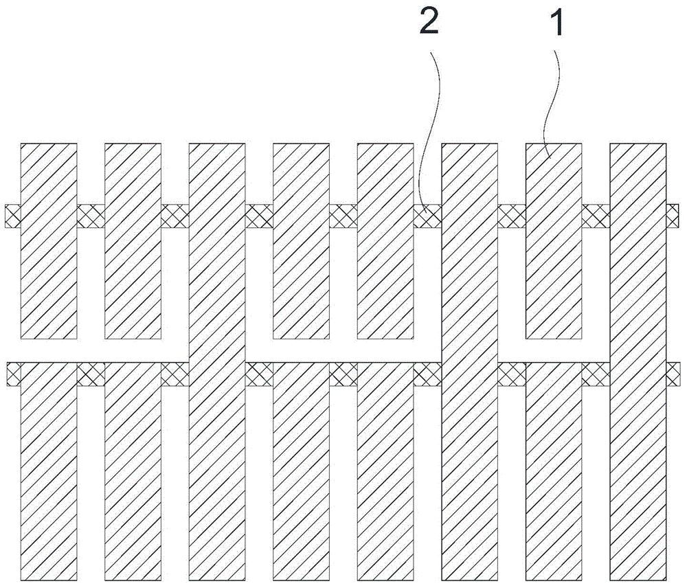
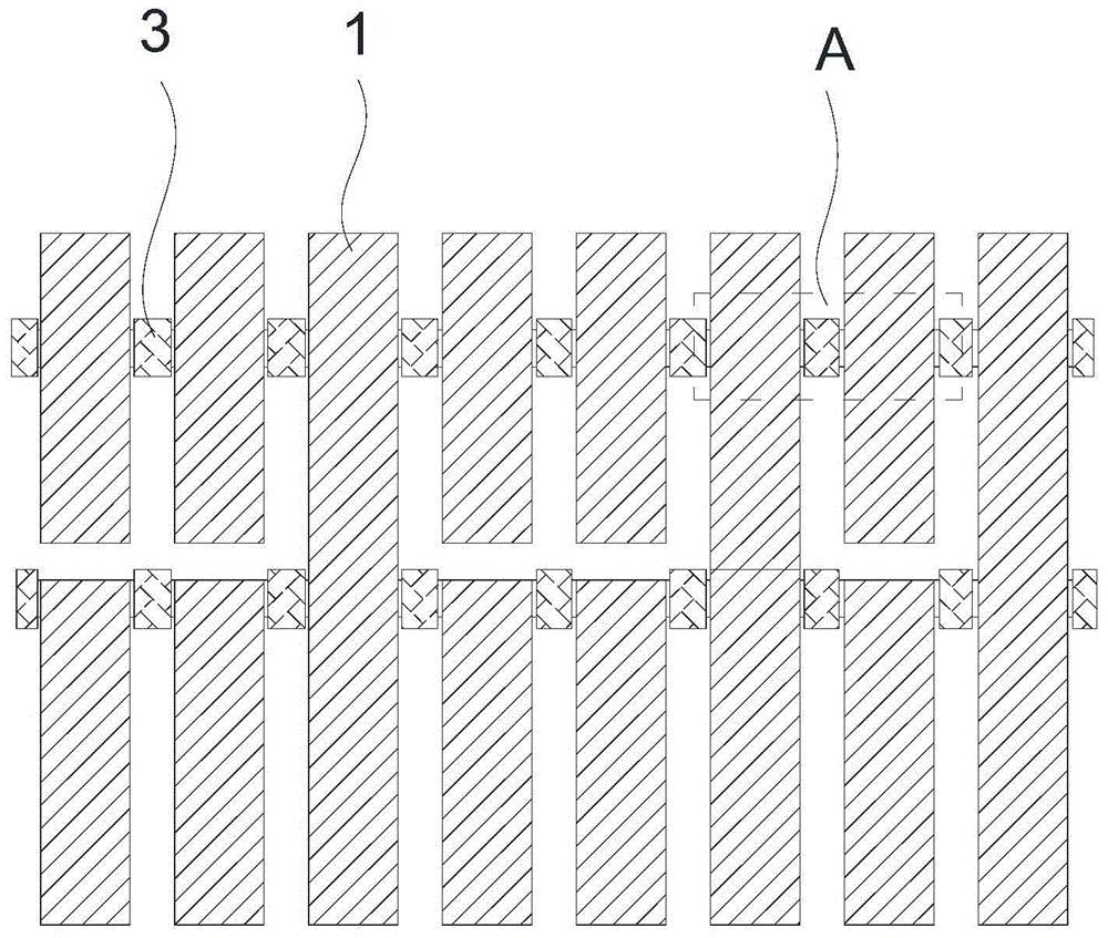
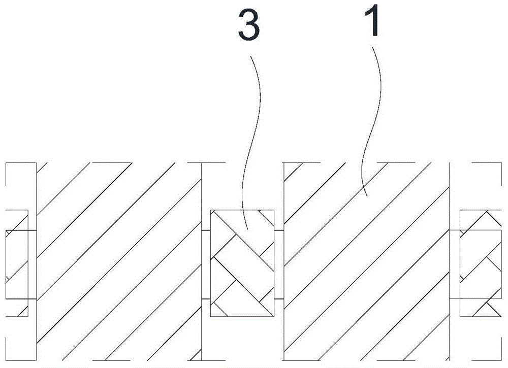
Image

Examples
Embodiment
[0020] PCB parameter requirements
[0021] Inner core board:
[0022] 0.075mm 1 / 0.5OZ (without copper) (2 pieces);
[0023] 0.15mm 0.5 / 0.5OZ (without copper) (2 sheets);
[0024] 0.076mm 0.5 / 0.5OZ (without copper) (2 sheets);
[0025] Number of layers: 14 layers;
[0026] Inner line width / spacing: 0.089mm / 0.096mm, 0.096 / 0.096mm;
[0027] Outer layer line width / line spacing: 0.103 / 0.095mm (finished copper thickness 1.0OZ);
[0028] Sheet Tg: ≥170°;
[0029] Outer copper foil: 1 / 3OZ;
[0030] Hole copper thickness: 20μm(min) / 25μm(ave);
[0031] Surface treatment: immersion gold + electric gold fingers;
[0032] Finished board thickness: 1.6mm±10%;
[0033] Minimum drill bit: 0.25mm;
[0034] Drilling thickness to diameter ratio: 6.4:1;
[0035] Production PNL size: 518mm×620mm.
[0036] The above-mentioned PCB manufacturing process including the golden finger manufacturing method of the present invention
[0037] 1. Cutting - According to the number of core boards w...
PUM
| Property | Measurement | Unit |
|---|---|---|
| thickness | aaaaa | aaaaa |
| thickness | aaaaa | aaaaa |
| thickness | aaaaa | aaaaa |
Abstract
Description
Claims
Application Information