Fixture for packaging stack array of semiconductor laser

A laser and semiconductor technology, which is applied in the direction of semiconductor lasers, lasers, laser components, etc., can solve the problems of reduced packaging accuracy, reduce errors, improve yield and reliability

Active Publication Date: 2015-09-23
ZHENGZHOU UNIV
View PDF6 Cites 6 Cited by
  • Summary
  • Abstract
  • Description
  • Claims
  • Application Information

AI Technical Summary

Problems solved by technology

[0004] The object of the present invention is to provide a jig for stack packaging of semiconductor lasers that prevents the placement of transi...

Method used


Image

  • Fixture for packaging stack array of semiconductor laser
  • Fixture for packaging stack array of semiconductor laser
  • Fixture for packaging stack array of semiconductor laser

Examples


Embodiment Construction

[0026] Attached below Figure 1~8 The present invention will be further described in detail with specific embodiments.

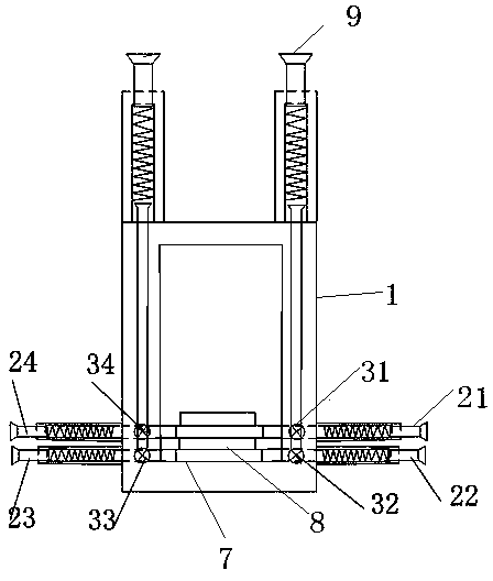
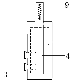
[0027] The present invention is a fixture for fixing and positioning the transitional heat sink of semiconductor laser stack package, including two guide rails fixed on the same fixed plate and a peg for fixing the transitional heat sink placed in the middle of the two guide rails. The studs are installed on the tracks of the two guide rails one by one. There are at least two studs. The studs include a pipe body. Movable screws and thimbles are respectively installed at both ends of the pipe body. The spring located between the screw and the thimble, when the screw is turned, the spring compresses and drives the thimble to move forward. The outer side of the end of the pipe body where the thimble is installed has a protrusion that can hold the peg in the track. The two tracks are fixed on the fixed plate. A transitional heat sink is fixed by two oppo...


PUM


Abstract

The invention provides a fixture for packaging a stack array of a semiconductor laser. The fixture comprises two guide rails fixed on a fixed plate, and at least two toggle pins used for fixing transition heat sinks placed in the middles of the two guide rails, wherein the toggle pins are mounted on tracks of the two guide rails in a one-to-one correspondence manner, and comprise tube bodies; movable screws and ejector pins are mounted at the two ends of the tube bodies respectively; the ejector pins move forward by screwing the screws; and the ejector pins of the two toggle pins in the one-to-one correspondence manner face towards the middles of the two guide rails. The fixture can realize positioning and fixing of the transition heat sinks in a packaging process, and can avoid displacement of the transition heat sinks and chips due to movement in the packaging process.

Description

technical field [0001] The invention relates to a device for packaging a stack of lasers, in particular to a fixture for packaging a stack of semiconductor lasers. Background technique [0002] The semiconductor laser array chip is composed of many semiconductor laser light-emitting units, and these light-emitting units form an array chip (Bar bar) on a chip that has not been cleaved. Then, these array chips are vertically stacked and packaged by a certain method to form a semiconductor laser stack. In this way, multiple array chips are packaged together, and multiple array chips work at the same time to achieve high-power laser output. Semiconductor laser stack packaging is very difficult, because the array chips (bars) of semiconductor lasers are very small, with a thickness of about 0.5 mm, a length of about 10 mm, and a width of about 1 mm. At present, there is no fully automatic equipment that can directly package the stack. Therefore, at present, the packaging o...

Claims


Application Information

Patent Timeline
IPC IPC(8): H01S5/022
Inventor 程东明
Owner ZHENGZHOU UNIV
Why Eureka
Try Eureka