Test method of parallel quadrilateral LED chip

A LED chip and parallelogram technology, which is applied in the testing field of parallelogram LED chips, can solve the problems of inability to have one-to-one correspondence of photoelectric characteristics test data, cumbersome testing process of parallelogram LED chips, etc., so as to avoid failure to correspond one by one and solve production difficulties , The effect of simplifying the production process

Active Publication Date: 2015-10-07
XIAMEN SANAN OPTOELECTRONICS TECH CO LTD
View PDF4 Cites 0 Cited by
  • Summary
  • Abstract
  • Description
  • Claims
  • Application Information

AI Technical Summary

Problems solved by technology

[0003] The present invention provides a test method for LED chips, which solves the cumbersome test process of existing parallelogram LED chips and cannot directly compare the test data of photoelectric characteristics with the coordinate positions of the chip Corresponding problems, thus greatly improving test efficiency

Method used


Image

  • Test method of parallel quadrilateral LED chip
  • Test method of parallel quadrilateral LED chip
  • Test method of parallel quadrilateral LED chip

Examples


Embodiment 1

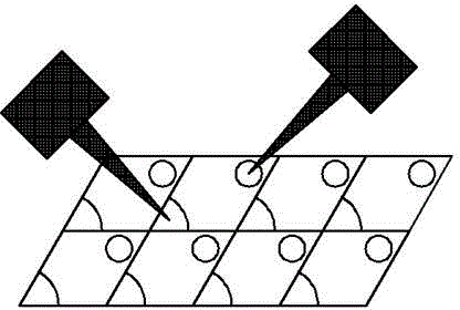
[0021] like figure 2 As shown, this embodiment provides a 4-pin point measurement method for a parallelogram LED chip, that is, a testing machine with 2 sets of probe modules is used to test the photoelectric characteristics of 2 chip units to be tested, and the probe modules simultaneously test 2 For adjacent chip units in the same row, the inner angles of the chip units are 60° and 120°. The test sequence and direction of the chip are shown by the arrows, first from left to right, then from top to bottom. When the next two rows of core particles (shaded slashes) are tested, a rectangular coordinate system is just formed, that is, the current spot measurement The two core particles and the two core particles of the lower oblique line are orthogonally translated, and the abscissas of the center points of the upper and lower adjacent chip units to be tested are consistent. At this time, the photoelectric characteristic parameters of the chip and the coordinate position of the...

Embodiment 2

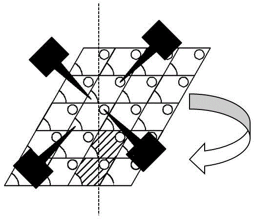
[0023] like image 3 As shown, this embodiment provides a 6-pin spot test method for a parallelogram LED chip, that is, a testing machine with 3 sets of probe modules is used to test the photoelectric characteristics of 3 chip units to be tested, and the probe modules simultaneously test 3 Adjacent chip units in the same line (the position where the probe module contacts the electrodes, not shown in the figure), the inner angles of the chip units are 45° and 135°. The test sequence and direction of the chip are shown by the arrows, first from left to right along the X axis, and then from top to bottom along the Y axis. The core grain and the two core grains with the oblique line below are orthogonally translated, and the abscissas of the center points of the upper and lower adjacent chip units to be tested (located in the dotted line box) are consistent. At this time, the photoelectric characteristic parameters of the chip and the coordinate position of the center point of th...

Embodiment 3

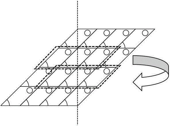
[0025] like Figure 4 As shown, different from Embodiment 2, this embodiment provides an 8-pin point measurement method for a parallelogram LED chip, that is, a testing machine with 4 sets of probe modules is used to test the photoelectric characteristics of 4 chip units to be tested. Its probe module tests 4 adjacent chip units (located in the dotted line box) at the same time, and the chip units to be tested are combined in 2×2 rows and columns, and the test time is shortened to 1 / 4.


PUM


Abstract

The invention relates to a test method of a parallel quadrilateral LED chip. According to the test method, the interior angles of a used parallel quadrilateral LED chip are specific angles; a test machine is provided with two or more groups of test pins, namely, a plurality of groups of test modules which can test specific two or more rows of chips simultaneously. With the test method adopted, the problem of incapability of realizing one-by-one correspondence of test data or the problem of incapability of a test system to find chips correctly can be solved.

Description

technical field [0001] The invention relates to semiconductor device testing, in particular to a testing method for parallelogram LED chips. Background technique [0002] Most of the existing LED semiconductor chips are rectangular. When the emission angle is greater than 23.5° and less than 66.5°, the light of the chip will only be reflected back and forth inside the chip, and the photons cannot escape from the outside of the chip, resulting in loss of light output from the chip. At present, the methods used to improve the light-emitting efficiency of LED chips include patterning the light-emitting surface of the LED chip, patterning the light-emitting sidewall of the LED chip, and deforming the shape of the LED chip (such as a parallelogram), etc. These technologies can be used to a certain extent. Improve the luminous efficiency of LED chips. However, although the design of parallelogram LED chips can improve the external quantum efficiency, since the chips are arranged i...

Claims


Application Information

Patent Timeline
Patent Type & Authority Applications(China)
IPC IPC(8): G01R31/26
Inventor 林潇雄邱树添林素慧彭康伟许圣贤
Owner XIAMEN SANAN OPTOELECTRONICS TECH CO LTD
Why Eureka
Try Eureka