Liquid crystal display device and common voltage compensation method thereof

A liquid crystal display device and public voltage technology, which is applied to static indicators, instruments, etc., can solve problems such as uneven distribution and affect the quality of picture display, achieve the same difference in public voltage, and improve the effect of picture display quality

Active Publication Date: 2017-05-10
KUSN INFOVISION OPTOELECTRONICS
View PDF5 Cites 1 Cited by
  • Summary
  • Abstract
  • Description
  • Claims
  • Application Information

AI Technical Summary

Problems solved by technology

[0004] The present invention provides a liquid crystal display device and a common voltage compensation method thereof, which solves the problems of the liquid crystal display device affecting the quality of picture display due to uneven distribution of common voltage at different positions

Method used


Image

  • Liquid crystal display device and common voltage compensation method thereof
  • Liquid crystal display device and common voltage compensation method thereof
  • Liquid crystal display device and common voltage compensation method thereof

Examples


no. 1 example

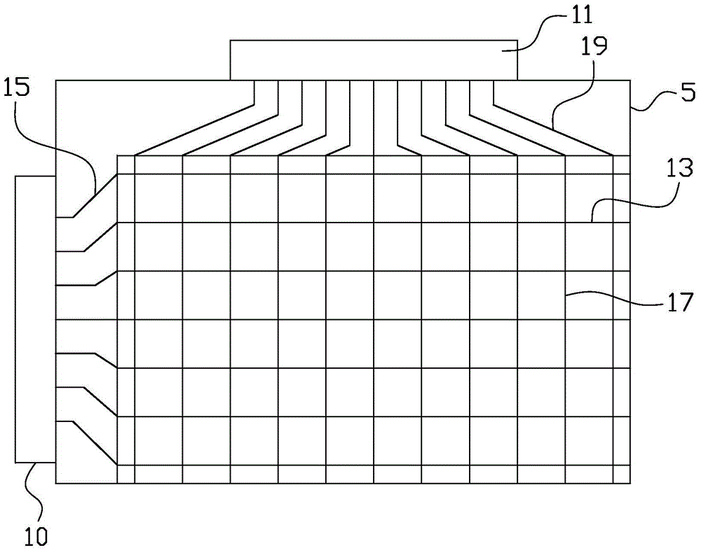
[0035] Figure 2A It is a flow chart of the public voltage compensation method provided by the first embodiment of the present invention. The common voltage compensation method is applicable to a liquid crystal display panel, and the liquid crystal display panel includes a plurality of gate lines and a plurality of data lines intersecting with the plurality of gate lines, please refer to Figure 2A , the public voltage compensation method of this embodiment includes the following steps 200-209.

[0036] Step 200, simulating m horizontal lines parallel to the gate lines and n vertical lines crossing the m horizontal lines and parallel to the data lines for the display area of ​​the liquid crystal display panel, and dividing the display area into n*m area, where m and n are integers greater than 0.

[0037] Such as Figure 2B As shown, it is assumed that the display area 220 of the liquid crystal display panel is divided into regions, m horizontal lines 221 parallel to the ga...

no. 2 example

[0053] Figure 3A is a flow chart of the common voltage compensation method provided by the second embodiment of the present invention. This embodiment and Figure 2A The difference is that in this embodiment, the lateral common voltage (influenced by the resistance-capacitance delay effect caused by the gate line) is compensated. The common voltage compensation method includes the following steps 300-309.

[0054] Step 300, simulating m horizontal lines parallel to the gate lines and n vertical lines crossing the m horizontal lines and parallel to the data lines for the display area of ​​the liquid crystal display panel, and dividing the display area into n*m area, where m and n are integers greater than 0.

[0055] This step is related to Figure 2A Step 200 is the same, and will not be repeated here.

[0056] The lateral common voltage compensation (influenced by the resistor-capacitor delay effect caused by the gate line) will be described below.

[0057] Step 301, s...

no. 3 example

[0071] Figure 4A is a flow chart of the common voltage compensation method provided by the third embodiment of the present invention. This embodiment and Figure 2A The difference is that in this embodiment, both the horizontal common voltage (influenced by the resistance-capacitor delay effect caused by the gate line) and the vertical common voltage are compensated. The common voltage compensation method includes the following steps 400-409.

[0072] Step 400, simulating m horizontal lines parallel to the gate lines and n vertical lines crossing the m horizontal lines and parallel to the data lines in the display area of ​​the liquid crystal display panel, and dividing the display area into n*m area, where m and n are integers greater than 0.

[0073] This step is related to Figure 2A Step 200 is the same, and will not be repeated here.

[0074] The horizontal common voltage compensation (influenced by the resistor-capacitor delay effect caused by the gate line) and th...


PUM


Abstract

The embodiment of the invention discloses a liquid crystal display device and a common voltage compensation method thereof, and belongs to the technical field of display. The common voltage compensation method comprises the steps that m transverse lines and n vertical lines are simulated in the display area of a liquid crystal display panel; common voltage of the m transverse lines is simulated, and gate and source electrode parasitic capacitance of the corresponding m transverse lines is obtained according to the simulated common voltage of the corresponding m transverse lines; the compensation capacitance value of the corresponding m transverse lines is obtained according to the calculated gate and source electrode parasitic capacitance of the corresponding m transverse lines; the common voltage of the corresponding m transverse lines is calculated again; and whether the difference value between the common voltage of the adjacent transverse lines is less than a standard value is judged, and the gate and source electrode parasitic capacitance of the liquid crystal display device is compensated according to the compensation capacitance value of the corresponding m transverse lines if the judgment result is yes so that the common voltage along the direction of the m transverse lines is enabled to be uniform in distribution. The common voltage along the direction of the m transverse lines is enabled to be uniform in distribution so that frame display quality is enhanced.

Description

technical field [0001] The invention relates to the field of display technology, in particular to a liquid crystal display device and a common voltage compensation method thereof. Background technique [0002] Liquid crystal display (Liquid Crystal Display, LCD) has the advantages of good image quality, small size, light weight, low driving voltage, low power consumption, no radiation and relatively low manufacturing cost. It currently dominates the field of flat panel display. Display devices are very suitable for use in desktop computers, palmtop computers, personal digital assistants (Personal Digital Assignment, PDA), portable phones, televisions, and various office automation and audio-visual equipment. [0003] The liquid crystal display panel is an important part of the liquid crystal display device. Figure 1A is a schematic diagram of a partial structure of an existing liquid crystal display panel, such as Figure 1A As shown, in the liquid crystal display panel 5, ...

Claims


Application Information

Patent Timeline
Patent Type & Authority Patents(China)
IPC IPC(8): G09G3/36
Inventor 李亚锋戴文君谢颖颖
Owner KUSN INFOVISION OPTOELECTRONICS
Why Eureka
Try Eureka