Pixel circuit and display device

A pixel circuit and capacitor technology, which is applied in the field of pixel circuits, can solve the problems of decreased aperture ratio and loss of brightness, etc., and achieve the effect of reducing the impact and prolonging the charging and discharging time

Active Publication Date: 2017-12-22
AU OPTRONICS CORP
View PDF4 Cites 0 Cited by
  • Summary
  • Abstract
  • Description
  • Claims
  • Application Information

AI Technical Summary

Problems solved by technology

Generally speaking, the storage capacitor 13 can help to stabilize the data potential stored in the liquid crystal capacitor 12, but when the operating frequency is higher such as Field Sequential (Field Sequential) display, or liquid crystal material with high dielectric coefficient such as blue phase liquid crystal, When a ferroelectric liquid crystal (Ferroelectric LC) display is used, a storage capacitor 13 with a larger capacitance value is needed to help stabilize the data potential stored in the liquid crystal capacitor 12, and this large-area storage capacitor 13 with a larger capacitance value will cause an aperture ratio ( Aperture Ratio) drops and loses brightness

Method used


Image

  • Pixel circuit and display device
  • Pixel circuit and display device
  • Pixel circuit and display device

Examples


Embodiment Construction

[0058] The present invention will be described in detail below in conjunction with the accompanying drawings and specific embodiments, but not as a limitation of the present invention.

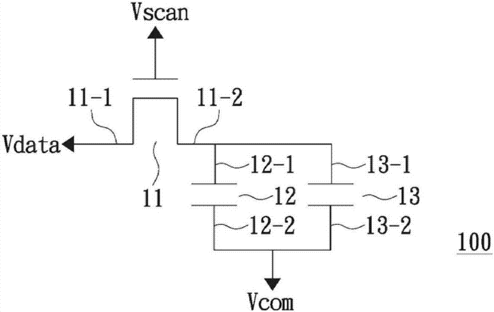
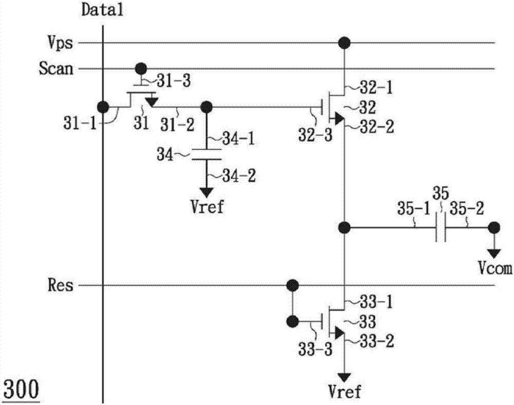
[0059] image 3 It is a circuit diagram of a pixel circuit according to an embodiment of the present invention. Such as image 3As shown, the pixel circuit 300 includes a scan line Scan, a first data line Data1 , a power line Vps, a reset line Res, a first transistor 31 , a second transistor 32 , a third transistor 33 , a first capacitor 34 and a liquid crystal capacitor 35 . The scan line Scan is used to provide a scan signal, the first data line Data1 is used to provide a first data signal, the power line Vps is used to provide power, and the reset line Res is used to provide a reset signal. The first transistor 31 has a first terminal 31-1, a second terminal 31-2 and a control terminal 31-3. The control terminal 31-3 of the first transistor 31 is electrically coupled to the scan line Sca...


PUM


Abstract

The invention relates to a pixel circuit comprising a first transistor, a second transistor, a third transistor, a first capacitor and a liquid crystal capacitor. A control terminal of the first transistor receives scanning signals, and a first terminal of the first transistor receives first data signals. A first terminal of the first capacitor is electrically coupled to a second terminal of the first transistor, and a second terminal of the first capacitor receives reference potential. A control terminal of the second transistor is electrically coupled to a first terminal of the liquid crystal capacitor, and a second terminal of the third transistor receives reference potential.

Description

technical field [0001] The present invention relates to a pixel circuit, in particular to a pixel circuit of a liquid crystal display device. Background technique [0002] figure 1 It is a circuit diagram of a pixel circuit of a conventional liquid crystal display device. Such as figure 1 As shown, the pixel circuit 100 includes a transistor 11 , a liquid crystal capacitor 12 and a storage capacitor 13 . The transistor 11 has a first terminal 11-1, a second terminal 11-2 and a control terminal 11-3. The control terminal 11-3 of the transistor 11 is used to receive the scan signal Vscan, the first terminal 11-1 of the transistor 11 is used to receive the data signal Vdata, and the second terminal 11-2 of the transistor 11 is electrically connected to the first terminal of the liquid crystal capacitor 12 12 - 1 and the first terminal 13 - 1 of the storage capacitor 13 , the second terminal 12 - 2 of the liquid crystal capacitor 12 and the second terminal 13 - 2 of the stor...

Claims


Application Information

Patent Timeline
Patent Type & Authority Patents(China)
IPC IPC(8): G02F1/1362G09G3/36
CPCG02F1/136213G02F1/136286G09G3/36
Inventor 谢嘉定洪嘉泽小泽德郎曾柏翔郭家玮
Owner AU OPTRONICS CORP
Why Eureka
Try Eureka