

a lead frame
A lead frame and gate technology, applied in the direction of semiconductor/solid-state device parts, semiconductor devices, electrical components, etc., can solve the problems of flip-chip scrapped products, increased manufacturing costs, and difficult manufacturing processes, so as to avoid product scrapping, Facilitate the effect of subsequent manufacturing
- Summary
- Abstract
- Description
- Claims
- Application Information
AI Technical Summary
Problems solved by technology
Method used
Image

Examples
Embodiment 1
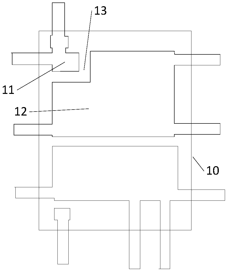
[0027] Figure 2a with 2b A structural diagram of a lead frame provided by Embodiment 1 of the present invention is shown. Such as Figure 2a As shown, the lead frame 20 (used to flip-chip a rectangular chip) includes a gate pad 21 , a source pad 22 and a gate isolation strip 23 between the gate pad 21 and the source pad 22 . The gate isolation strip 23 is used to electrically insulate the gate pad 21 from the source pad 22 . The lead frame 20 is also provided with a balance slot 24a opposite to the gate isolation strip 23, and the balance slot 24a is used to balance the uneven stress caused by the gate isolation strip 23 during chip flipping. Specifically, the balance groove 24a is located on the diagonal line of the chip flip-chip area, and the balance groove 24a and the gate isolation strip 23 are respectively located at both ends of the diagonal line of the chip flip-chip area, that is, the gate isolation strip 23 and the The balance groove 24 a is arranged symmetrical...
Embodiment 2
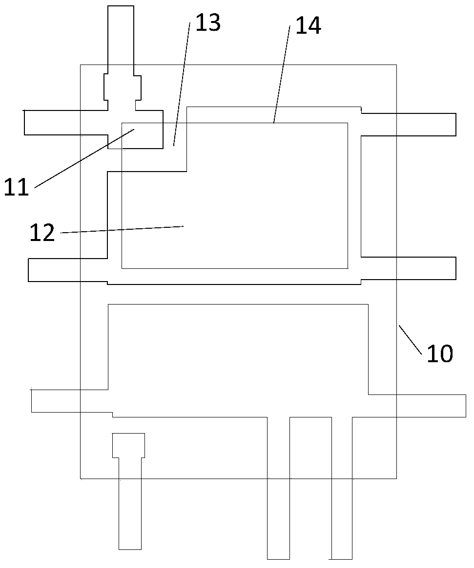
[0031] Figure 3a with 3b A structural diagram of another lead frame provided by Embodiment 2 of the present invention is shown. Similar to Embodiment 1, in the source bonding region 22 of the lead frame 20 for flip-chip rectangular chips, a balance groove 24b is provided on the diagonal of the chip flip-chip region, and the balance groove 24b and the gate isolation strip 23 are respectively Located at both ends of the same diagonal line, that is, the gate isolation strip 23 and the balance groove 24 b are arranged symmetrically with respect to the center of the flip-chip area on the lead frame 20 . The balance groove 24b is formed by connecting one end of the first etching groove 24b1 and the second etching groove 24b2 whose included angle is a right angle. The balance groove 24b is a non-local etching groove, that is, the balance groove 24b divides the source welding region 22 into two parts. In addition, the width of the balance groove 24b is equal to the width of the ga...
Embodiment 3
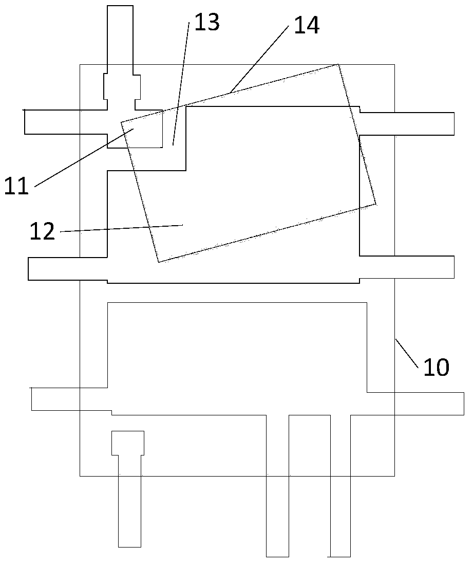
[0034] Figure 4a A structural diagram of another lead frame provided by Embodiment 3 of the present invention is shown. A balance groove 24c is provided on the source pad 22 of the lead frame 20 for flip-chip rectangular chips. The balance groove 24c is formed by connecting one end of the first etching groove 24c1 and the second etching groove 24c2 with an acute angle. The balance groove 24c is a partially etched groove. In addition, the position of the balance groove 24c is on the diagonal of the chip flip-chip area, and away from the gate isolation zone 23, the width is smaller than the width of the gate isolation zone 23, and the etching depth is 1 / of the thickness of the lead frame 20. 3 (such as Figure 4b shown).
[0035] It is worth noting that, in the first embodiment, the angle between the first etching groove and the second etching groove is a right angle, and the width of the balancing groove is equal to the width of the gate isolation strip. In the third emb...
PUM
 Abstract
Description
Claims
Application Information