Grid electrode protection circuit for field effect transistors connected in series

A field effect tube and protection circuit technology, which is applied in the field of field effect tube series gate protection circuit, can solve the problems of gate voltage overrun, field effect tube breakdown, etc., and achieve the effect of improving the high voltage resistance range

Inactive Publication Date: 2015-10-28
绍兴合田新能源有限公司
View PDF8 Cites 0 Cited by
  • Summary
  • Abstract
  • Description
  • Claims
  • Application Information

AI Technical Summary

Problems solved by technology

[0004] The purpose of the present invention is to provide a field effect transistor series gate protection circuit, in order to solve the problem that the field effect transistor is broken down when the gate voltage exceeds the limit when the field effect transistor is connected in series

Method used


Image

  • Grid electrode protection circuit for field effect transistors connected in series
  • Grid electrode protection circuit for field effect transistors connected in series

Examples


Embodiment 1

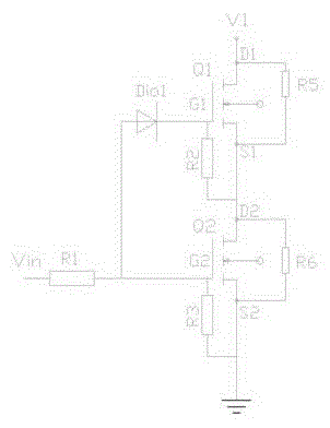
[0011] like figure 1 As shown, a field effect transistor series gate protection circuit, the field effect transistor control voltage Vin is connected in series with the gate G1 of the field effect transistor Q1 through the diode Dio1.

[0012] When the FET control voltage Vin is at a high level greater than the Vth of the FET, the FET Q1 and the FET Q2 are turned on, and the voltage V1 between the drain D1 of the FET Q1 and the S2 source of Q2 is close to at zero.

[0013] When the FET control voltage Vin is zero, the FET Q1 and the FET Q2 are turned off, and the voltage between the drain D1 of the FET Q1 and the S2 source of the FET Q2 is V1. R5 and R6 are equalizing resistors, VR5=VR6, VR5+VR6= V1. When V1 is high, if the diode Dio1 is not connected, VS1G1 may exceed the gate voltage limit of the field effect transistor Q1, and the field effect transistor Q1 will be broken down. After the diode Dio1 is connected, due to the blocking function of the diode, VS1G1 is zero, a...

Embodiment 2

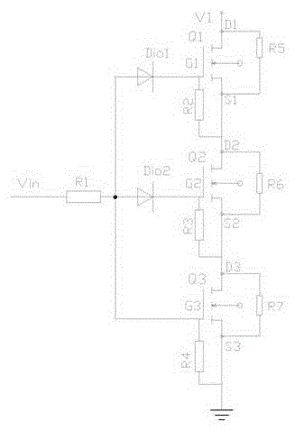
[0016] like figure 2 As shown, the field effect transistor control voltage Vin is connected in series to the gate G1 of the field effect transistor Q1 and the gate G2 of the field effect transistor Q2 through the diode Dio1 and the diode Dio2 respectively.

[0017] When the FET control voltage Vin is at a high level greater than the Vth of the FET, the FET Q1, the FET Q2, and the FET Q3 are turned on, and the connection between the drain D1 and the source S1 of the FET Q1 is The voltage, the voltage between the drain D2 and the source S2 of the field effect transistor Q2, and the voltage between the drain D3 and the source S3 of the field effect transistor Q3 are all close to zero.

[0018] When the FET control voltage Vin is zero, the FET Q1, FET Q2, and FET Q3 are turned off, and the voltage between the drain D1 of the FET Q1 and the S3 source of the FET Q3 is VD1S3= V1. R5, R6, R7 are voltage equalizing resistors, VR5=VR6= VR7, VR5+VR6+ VR7= V1, when V1 is high, if diode...


PUM


Abstract

The invention discloses a grid electrode protection circuit for field effect transistors connected in series. The grid electrode protection circuit comprises a circuit formed by series connection of more than one field effect transistor, grid electrodes of the field effect transistors are connected with a diode in series, a negative electrode of the diode is connected with the grid electrodes of the field effect transistors, a positive electrode of the diode is connected with a grid electrode control signal input terminal provided by the circuit in a unified manner, an equalizing resistor is connected between a drain electrode and a source electrode of each field effect transistor in parallel, and a voltage-releasing resistor is connected between the grid electrode and the source electrode of each field effect transistor in parallel. According to the circuit formed by series connection of more than one field effect transistor, the grid electrode of each field effect transistor is connected with one diode in series except for the grid electrode of the field effect transistor at a grounding terminal so that the problem that when the field effect transistors connected in series are turned off, the grid voltage is above the limit and causes breakdown is solved, the high-voltage-resistant range of the field effect transistors is extended, and the circuit can be widely applied in the photovoltaic, wind energy, and power electronics fields.

Description

technical field [0001] The invention relates to the field of electronic engineering, in particular to a field effect transistor series grid protection circuit. Background technique [0002] When the field effect tube is used as a switch, when the source and drain are disconnected, the voltage at both ends will increase. In some applications, the voltage between the source and drain will exceed its own withstand voltage limit. In order to solve this problem, it is necessary to replace the field effect tube with a higher withstand voltage, but this will cause some problems, such as the increase of power consumption non-linearity, the heating of the field effect tube will increase, the conduction voltage will increase, and there will be no higher withstand voltage. Field effect tubes are available for selection. In the face of these problems, only multiple FETs can be used in series to improve the overall withstand voltage level when they are turned off. [0003] After multip...

Claims


Application Information

Patent Timeline
Patent Type & Authority Applications(China)
IPC IPC(8): H02M1/32H03K17/08
CPCY02E10/56
Inventor 张宗威张夏张朝宫
Owner 绍兴合田新能源有限公司
Why Eureka
Try Eureka