An organic optoelectronic device

An optoelectronic device and organic technology, applied in the field of organic optoelectronic devices, can solve the problems of short burnout time, screen burnout, OLED screen burnout, etc., and achieve the effect of improving service life and improving bearing capacity.

Active Publication Date: 2022-07-19
GUAN YEOLIGHT TECH CO LTD
View PDF6 Cites 0 Cited by
  • Summary
  • Abstract
  • Description
  • Claims
  • Application Information

AI Technical Summary

Problems solved by technology

[0006] The working voltage of the OLED screen is constant, generally 4-5V, and when there is a circuit failure, the voltage will rise, the OLED screen will become very bright, and then the OLED screen will be burned out, and the voltage will exceed the safety limit. The higher the voltage, the shorter the time from when the OLED screen is highlighted to burning out; therefore, generally OLEDs have a safe voltage, and the safety voltage of different OLED screens varies according to the device structure. Generally, when the voltage of the OLED screen is greater than the safe voltage After a period of time, the screen body will be burned

Method used


Image

  • An organic optoelectronic device
  • An organic optoelectronic device
  • An organic optoelectronic device

Examples


Embodiment 1

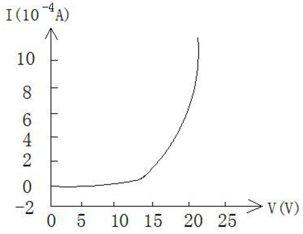
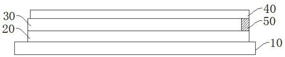
[0038] Please refer to figure 2 , this embodiment provides an organic optoelectronic device, comprising a substrate 10, and a first electrode layer 20, an organic functional layer 30 and a second electrode layer 40 formed on the substrate 10 in sequence; the first electrode layer 20 and Between the second electrode layers 40, an over-electricity confinement layer 50 is arranged in parallel with the organic functional layer 30, and the material of the over-electricity confinement layer 50 is a pressure-sensitive material.

[0039] The over-electric confinement layer, its varistor voltage V 压敏 with the safe voltage V of organic optoelectronic devices 安全 The relationship is as follows:

[0040] V 压敏 =k*V 安全, k is a constant between 0.7-1.3;

[0041] where the safety voltage V 安全 It is set according to different device structures, which is generally related to the operating voltage V of the organic optoelectronic device. 0 The following relationship is satisfied between: ...

Embodiment 2

[0082] On the basis of Example 1, the implementation of the over-electricity confinement layer 50 in this example is replaced by: directly using the insulating region in the organic optoelectronic device to realize, specifically:

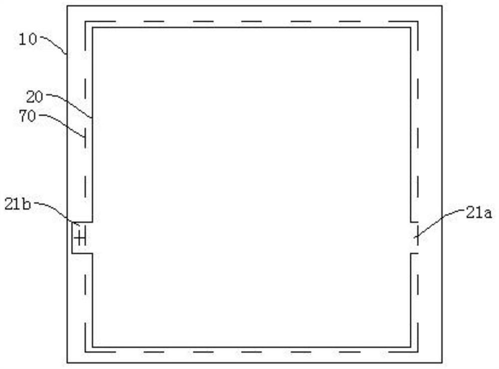
[0083] like Figure 15 As shown, taking the OLED screen as an example, in the structure of the OLED device, an insulating region 60 is provided between the first electrode layer 20 and the second electrode layer 40; the insulating region 60 is formed on the first electrode layer 40. On the electrode layer 20 and it isolates the pixel area on the first electrode layer 20, the organic functional layer 30 is located in the pixel area; the insulating area 60 is used to isolate the first electrode layer 20 and the second electrode layer 40 is also used to isolate adjacent pixels; it is generally selected from organic materials, such as phenolic resin, polyimide, etc.; in this embodiment, the material of the entire area of ​​the insulating region 60 is di...


PUM

PropertyMeasurementUnit
thicknessaaaaaaaaaa

Abstract

The present application discloses an organic optoelectronic device, comprising a substrate, and a first electrode layer, an organic functional layer and a second electrode layer sequentially formed on the substrate; There is an over-electric confinement layer in parallel with the organic functional layer, and the over-electric confinement layer is formed of a pressure-sensitive material. In the present application, an over-electricity limiting layer connected in parallel with the organic functional layer is provided between the first electrode layer and the second electrode layer of the organic optoelectronic device. The resistance of the electrical confinement layer becomes smaller, allowing the current to pass through the over-electric confinement layer without damaging the organic optoelectronic device. When the voltage returns to normal, the resistance of the over-electric confinement layer returns to infinity, and the organic optoelectronic device can work normally.

Description

technical field [0001] The present disclosure relates to the technical field of organic optoelectronics, and in particular, to an organic optoelectronic device. Background technique [0002] Organic optoelectronics is an emerging research field formed by the intersection of many disciplines such as organic chemistry, physics, information electronics science and materials science. In particular, organic optoelectronic functional materials and devices represented by organic electroluminescent devices (OLEDs), organic photovoltaics (OPVs) and organic field effect transistors (OTFTs) are used in new flat panel displays, solid-state lighting, high-density information transmission and storage, The fields of new energy and photochemistry have shown broad application prospects, and have received widespread attention from the scientific and industrial circles. For example, OLED technology has many advantages such as all-solid-state, active light-emitting, rich colors, and flexible d...

Claims


Application Information

Patent Timeline
Patent Type & Authority Patents(China)
IPC IPC(8): H01L27/32H01L51/52
CPCH10K59/12H10K59/126H10K50/80
Inventor 郭立雪许显斌谢静赵杨苏乃文
Owner GUAN YEOLIGHT TECH CO LTD
Why Eureka
Try Eureka