Touch display panel, manufacturing method and repairing method thereof

A technology of a touch display panel and a manufacturing method, which are applied in the directions of instruments, electrical digital data processing, and data processing input/output processes, etc., can solve problems such as reducing the aperture ratio of a display device, and achieve the effect of reducing the influence of the aperture ratio.

Inactive Publication Date: 2018-09-11
BOE TECH GRP CO LTD +1
View PDF3 Cites 2 Cited by
  • Summary
  • Abstract
  • Description
  • Claims
  • Application Information

AI Technical Summary

Problems solved by technology

Since both the first touch electrode 15 and the second touch electrode 23 need to occupy the area of ​​the light-transmitting region, the aperture ratio of the display device will be reduced.

Method used


Image

  • Touch display panel, manufacturing method and repairing method thereof
  • Touch display panel, manufacturing method and repairing method thereof
  • Touch display panel, manufacturing method and repairing method thereof

Examples


Embodiment 1

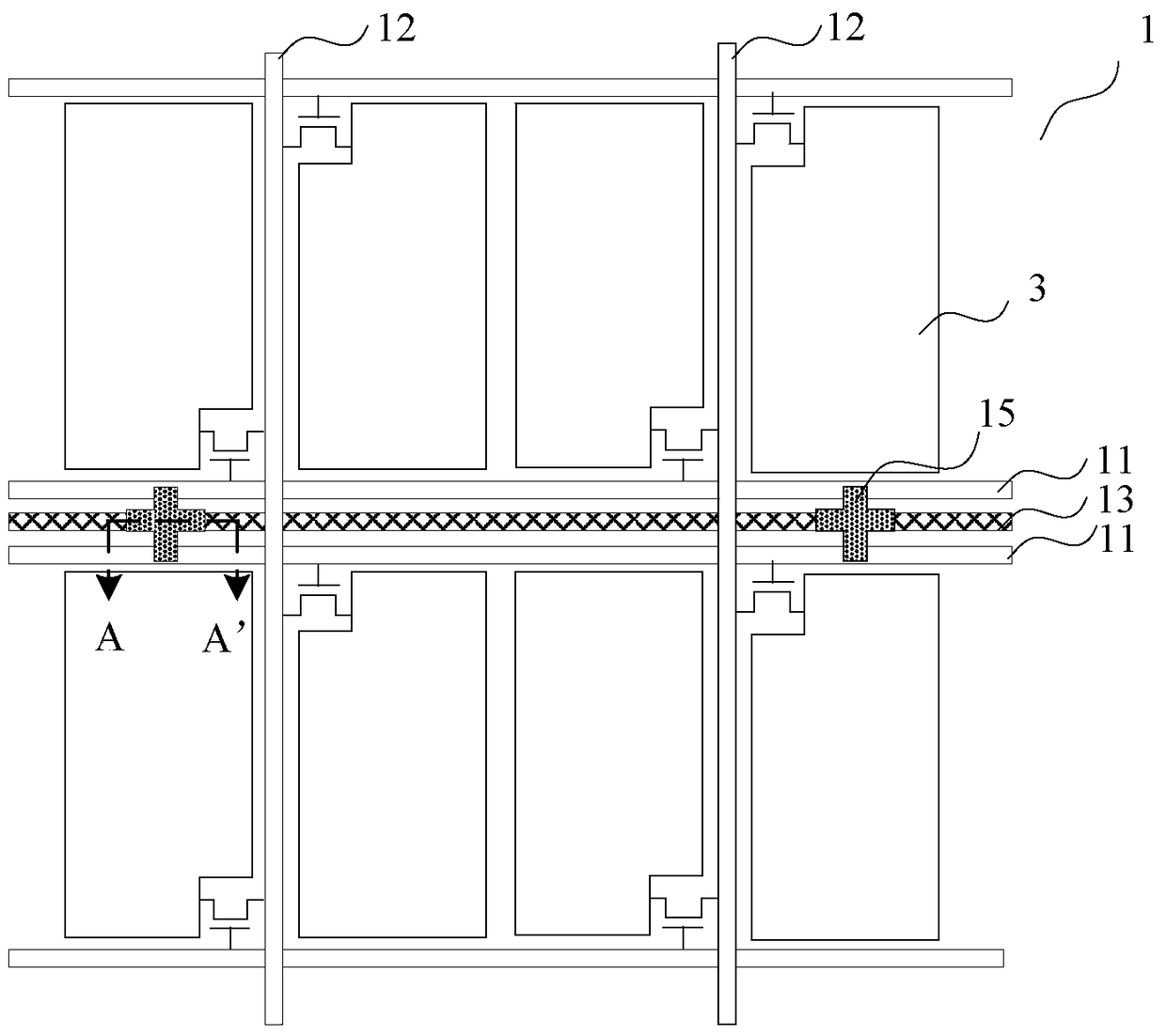
[0035] An embodiment of the present invention provides a touch display panel, such as Figure 2-Figure 7 As shown, the touch display panel includes a first substrate 1 and a second substrate 2 that are oppositely arranged. The first substrate 1 includes a plurality of first signal lines 11 parallel to each other and a plurality of second signal lines 12 parallel to each other. The first signal line 11 and the second signal line 12 are intersected and insulated.

[0036] The first substrate 1 further includes a plurality of first touch electrode traces 13 parallel to the first signal traces 11, and an insulating layer 14 and a first touch electrode 15 sequentially arranged on the first touch electrode traces 13, The insulating layer 14 is provided with a via hole 16 corresponding to the first touch electrode 15 , and the first touch electrode 15 is electrically connected to the first touch electrode wire 13 through the via hole 16 .

[0037]The second substrate 2 includes a se...

Embodiment 2

[0058] An embodiment of the present invention provides a method for manufacturing a touch display panel, the following combination Figure 2-Figure 7 The shown touch display panel describes the manufacturing method, which includes: the step of forming the first substrate 1 and the step of forming the second substrate 2, wherein:

[0059] The step of forming the first substrate 1 includes: forming a plurality of first signal lines 11 parallel to each other and a plurality of second signal lines 12 parallel to each other, and the first signal lines 11 and the second signal lines 12 are intersected and insulated.

[0060] The step of forming the first substrate 1 further includes: forming a first touch electrode wiring 13 parallel to the first signal line 11 , and sequentially forming an insulating layer 14 and a first touch electrode on the first touch electrode wiring 13 15 , wherein the insulating layer 14 is provided with a via hole 16 corresponding to the first touch electro...

Embodiment 3

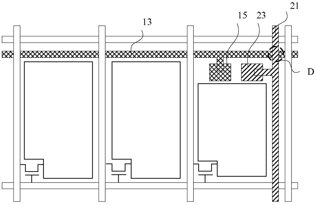
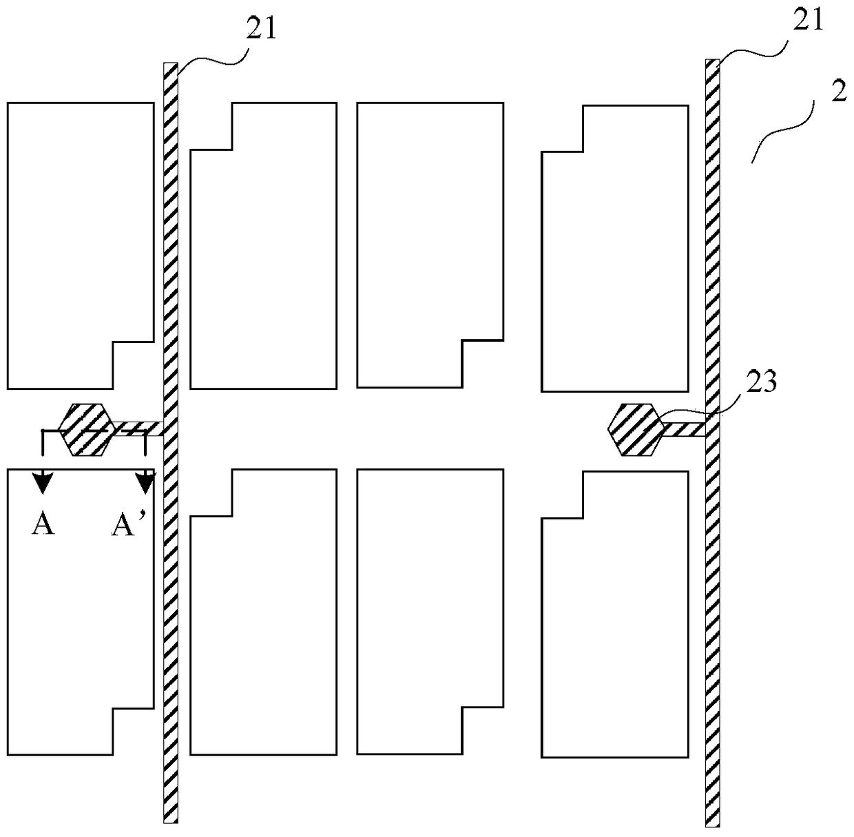
[0077] An embodiment of the present invention provides a method for repairing a touch display panel. The touch display panel has the structure in Embodiment 1. It should be emphasized that the first touch electrode 15 and the first touch electrode 15 in the touch display panel The first signal lines 11 adjacent to the first touch electrode traces 13 are partially overlapped, such as Figure 8 and Figure 9 As shown, the repair method includes: if the first signal line is disconnected, cutting the first touch electrode 11 on the outside of the first touch electrode 11 located at the two ends of the first signal line disconnection, and connecting the first touch electrode The overlapping portion of the control electrode 15 and the first signal line 11 is connected to the first signal line 11 .

[0078] Since when the first signal line 11 is disconnected, the first touch electrode trace 13 is cut off outside the first touch electrode 15 located at both ends of the disconnection ...


PUM


Abstract

The invention discloses a touch display panel, a manufacturing method of the touch display panel and a restoring method of the touch display panel, and relates to field of display technologies. Influences on the aperture ratio of a display device can be reduced. The touch display panel comprises a first substrate and a second substrate. The first substrate comprises first signal lines, second signal lines, a first touch electrode line, an insulating layer and first touch electrodes, and via holes corresponding to the first touch electrodes are formed in the insulating layer. The second substrate comprises second touch electrode lines, auxiliary spacers and second touch electrodes, the second touch electrodes at least partially cover the top ends, facing the first substrate, of the auxiliary spacers, the second touch electrodes are electrically connected with the second touch electrode lines, and the projections, on the first substrate, of the second touch electrodes and the first touch electrodes at least partially overlap. The touch display panel can be applied to the display device.

Description

technical field [0001] The invention relates to the field of display technology, in particular to a touch display panel, a manufacturing method and a repairing method thereof. Background technique [0002] With the development of display technology, the application of touch screen is more and more extensive. As an important type of touch screen, an in-cell touch screen (In Cell Touch Panel) can reduce the power consumption of the display device and make the display device thinner by integrating the touch electrodes on the array substrate of the display device. [0003] Such as figure 1 As shown, in the existing in-cell touch screen, the first touch electrode wiring 13, the first touch electrode 15, the second touch electrode wiring 21 and the second touch electrode 23 are arranged on the array substrate; wherein, Both the first touch electrodes 15 and the second touch electrodes 23 are located in the pixel unit area, and when the touch display panel is touched, the first t...

Claims


Application Information

Patent Timeline
Patent Type & Authority Patents(China)
IPC IPC(8): G06F3/041
Inventor 陈曦刘耀刘正张治超刘明悬张小祥
Owner BOE TECH GRP CO LTD
Why Eureka
Try Eureka