Circuit structure for high-density printed circuit board (PCB)

A technology of PCB board and circuit structure, which is applied in the computer field to achieve the effect of saving PCB area and facilitating testing

Inactive Publication Date: 2015-11-11
陈建国
View PDF0 Cites 2 Cited by
  • Summary
  • Abstract
  • Description
  • Claims
  • Application Information

AI Technical Summary

Problems solved by technology

[0003] The main purpose of this application is to provide a circuit structure for high-density PCB boards, aiming to solve the problems mentioned in the background technology

Method used


Image

  • Circuit structure for high-density printed circuit board (PCB)

Examples


Embodiment Construction

[0010] In order to make the purpose, principle and advantages of the present application clearer, the present application will be further described in detail below in conjunction with the accompanying drawings and embodiments. It should be understood that the specific embodiments described here are only used to explain the present application, and are not intended to limit the present application.

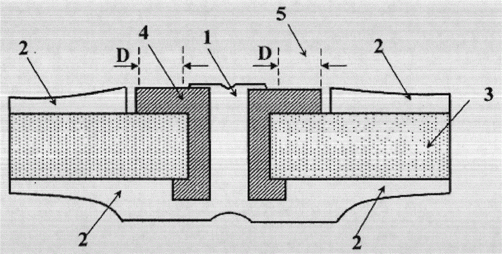
[0011] In the embodiment of the present application, aiming at the circuit structure of the high-density PCB board, it includes ball grid array packaged electronic devices, and a measuring point is set at the via hole position of the PCB wiring area below the ball grid array packaged electronic device; The PCB around the conductor layer at one end of the hole is covered by a solder resist layer, and the via hole is fully plugged by the solder resist layer and exposes the outer ring part of the conductor layer at one end of the via hole to form the measuring point; the via hole The ...


PUM


Abstract

The invention is suitable for the field of computers, and provides a circuit structure for a high-density printed circuit board (PCB). The circuit structure comprises a ball grid array-packaged electron device, wherein a measuring point is arranged at the position of a through hole in a PCB wiring region below the ball grid array-packaged electron device; the PCB around a conductor layer at one end of the through hole is covered with a solder resist layer; the through hole is fully filled with the solder resist layer and is exposed out of the outer ring part of the conductor layer at one end of the through hole to form the measuring point; and the conductor layer at the other end of the through hole and the PCB around the conductor layer are covered with the solder resist layer. According to the circuit structure, the measuring point is arranged in the through hole in the back surface of a ball grid array (BGA) electron device, so that the area of the PCB is reduced under the condition that the PCB is finite in area and relatively high in integration level; testing of a circuit is facilitated; and meanwhile, the signal quality of a PCB circuit is not affected.

Description

technical field [0001] The application belongs to the field of computers, and in particular relates to a circuit structure for high-density PCB boards. Background technique [0002] In the PCB circuit, in order to improve the product yield and verify the performance of the product, the test link of the PCB circuit board is indispensable. For the electronic devices packaged in BGA (BallGridArray, Ball Grid Array) in the PCB circuit, the usual test method is to test the electronic device on the PCB board Set the measuring point on the board and pass the measuring point to complete the measurement of the main signal. However, with the increase in the integration of electronic products, the electronic devices and wiring per unit area of ​​the PCB board are becoming more and more dense, and the requirements for signal quality and speed are becoming more and more stringent. Since each measuring point will occupy a certain area of ​​the PCB circuit board, circuit designers are not...

Claims


Application Information

Patent Timeline
IPC IPC(8): H05K1/02
CPCH05K1/0268
Inventor 陈建国
Owner 陈建国
Why Eureka
Try Eureka