Patch antenna and patch antenna manufacturing method

A chip antenna and chip technology, applied in the field of communication, can solve the problem of low PCB space utilization

Active Publication Date: 2017-02-08
RUIJIE NETWORKS CO LTD
View PDF9 Cites 4 Cited by
  • Summary
  • Abstract
  • Description
  • Claims
  • Application Information

AI Technical Summary

Problems solved by technology

[0004] Embodiments of the present invention provide a patch antenna and a method for manufacturing a patch anten

Method used


Image

  • Patch antenna and patch antenna manufacturing method
  • Patch antenna and patch antenna manufacturing method
  • Patch antenna and patch antenna manufacturing method

Examples


Embodiment 1

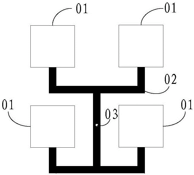
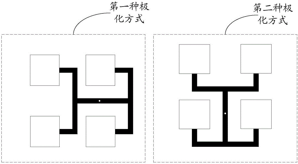
[0024] An embodiment of the present invention provides a patch antenna, which is applied to the above-mentioned communication equipment. Refer to Figure 4 As shown in , the patch antenna covers the PCB ( Figure 4 Not shown in ), the patch antenna includes: a first patch antenna array 61 and a second patch antenna array 62 . The first patch antenna array 61 includes M first patch elements 611 and a first feed network 612, and the second patch antenna array 62 includes N second patch elements 621 and a second feed network 622, M The first patch array 611 and the N second patch arrays 621 have L shared patch arrays 600, adjacent patch arrays belonging to the same patch antenna array are electrically connected to each other, and the first feed network 612 is along the first pole. The polarization direction is electrically connected to the first patch array 611 to form the first polarization mode; the second feed network 622 is electrically connected to the second patch array 62...

Embodiment 2

[0036] An embodiment of the present invention provides a method for manufacturing a patch antenna, referring to Figure 10 As shown in , this includes:

[0037] S101. Covering the first patch antenna array and the second patch antenna array on one side of the printed circuit board PCB, the first patch antenna array includes M first patch elements and a first feed network, and the second patch antenna array The antenna array includes N second patch elements and a second feed network, the M first patch elements and the N second patch elements have L common patch elements, and adjacent patches belonging to the same patch antenna array The chip arrays are electrically connected to each other, the first feed network is electrically connected to the M first chip arrays along the first polarization direction, and the second feed network is electrically connected to the N second chip arrays along the second polarization direction, The first polarization direction is different from th...


PUM


Abstract

The invention discloses a patch antenna and a patch antenna manufacturing method, which relate to the field of communication, and are used to solve the problem that the adoption of a dual-polarized antenna results in low PCB space utilization rate. The patch antenna comprises a first patch antenna array and a second patch antenna array. The first patch antenna array comprises M first patch dipoles and a first feed network. The second patch antenna array comprises N second patch dipoles and a second feed network. The M first patch dipoles and the N second patch dipoles share L patch dipoles. The adjacent patch dipoles belonging to the same patch antenna array are electrically connected with one another. The first feed network is electrically connected with the first patch dipoles along a first polarization direction, the second feed network is electrically connected with the second patch dipoles along a second polarization direction, and the first polarization direction is different from the second polarization direction. The embodiment of the invention is applied to the design of a dual-polarized patch antenna.

Description

technical field [0001] The present invention relates to the communication field, in particular to a patch antenna and a method for manufacturing the patch antenna. Background technique [0002] In the field of wireless communication, as the user environment becomes more complex, users have higher and higher requirements on the transmission rate. In this case, the requirement for the antenna is to provide a sufficiently high gain while satisfying the bandwidth. [0003] There are many ways to achieve high gain in antenna design, one of which is to use patch arrays. A patch array refers to an array composed of multiple patch antennas. The greater the number of patch arrays, the greater the antenna gain achieved. Such as figure 1 Shown is a polarized patch array composed of four patches, including patch 01, feed network 02, and feed point 03. However, dual-polarized antennas are generally used to transmit data in wireless communication systems to reduce the correlation betwe...

Claims


Application Information

Patent Timeline
IPC IPC(8): H01Q1/38H01Q1/50H01Q21/00H01Q21/24
CPCH01Q1/38H01Q1/50H01Q21/00H01Q21/24
Inventor 彭泽林
Owner RUIJIE NETWORKS CO LTD
Why Eureka
Try Eureka