Graphene-based spatial electro-optic modulator

An electro-optical modulator, graphene technology, applied in instruments, optics, nonlinear optics, etc., can solve the problems of large equivalent capacitance, modulation speed limitation, high electromagnetic loss, etc., to achieve small equivalent capacitance, easy integration, The effect of high modulation speed

Active Publication Date: 2018-12-28
XIAMEN UNIV
View PDF6 Cites 0 Cited by
  • Summary
  • Abstract
  • Description
  • Claims
  • Application Information

AI Technical Summary

Problems solved by technology

However, the disadvantage of the waveguide structure is that in order to achieve a large modulation depth, the waveguide must be long enough to enhance the interaction between graphene and the light field, which will increase the equivalent capacitance of the waveguide, thereby limiting the modulation speed. At the same time, there will be relatively high electromagnetic losses

Method used


Image

  • Graphene-based spatial electro-optic modulator
  • Graphene-based spatial electro-optic modulator
  • Graphene-based spatial electro-optic modulator

Examples


Embodiment Construction

[0022] The following embodiments will further illustrate the present invention in conjunction with the accompanying drawings.

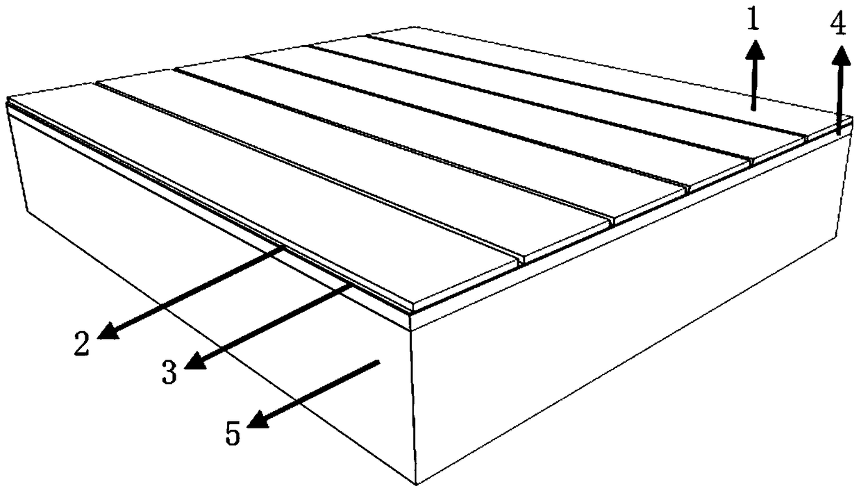
[0023] The following examples select a single-sided polished silicon wafer as the substrate, evaporate 150nm silver on the substrate by electron beam evaporation, deposit 16nm hBN on the Ag by radio frequency magnetron sputtering, and then use the method of chemical deposition , let graphene grow on hBN, and then use plasma chemical deposition method to form 1nm hBN on graphene. Finally, the silver bar block on the top layer is obtained by nanoimprinting method.

[0024] What the present invention adopts is metal layer-dielectric layer-metal layer (Metal-Dielectric-Metal) structure, and its composition sees figure 1 .

[0025] The present invention has a 5-layer structure, with an upper silver layer 1, an upper hexagonal boron nitride (hBN) layer 2, a graphene monoatomic layer 3, a lower hexagonal boron nitride (hBN) layer 4 and a lower silver layer...


PUM

PropertyMeasurementUnit
lengthaaaaaaaaaa
widthaaaaaaaaaa
thicknessaaaaaaaaaa

Abstract

The invention discloses a space electrooptical modulator based on graphene, and relates to an electrooptical modulator. The space electrooptical modulator adopts a five-layer structure and is provided with an upper silver layer, an upper hexagonal boron nitride layer, a graphene single-atom layer, a lower hexagonal boron nitride layer and a lower silver layer in sequence from top to bottom, wherein at least one slit is formed in the upper silver layer; the upper silver layer, the upper hexagonal boron nitride layer, the graphene single-atom layer, the lower hexagonal boron nitride layer and the lower silver layer are 200-300nm in length and 140-170nm in width; the upper silver layer is 10-30nm in thickness; the slits are 5-20nm in width; the upper hexagonal boron nitride layer is 1nm in thickness; the graphene single-atom layer is 0.3-0.8nm in thickness; the lower hexagonal boron nitride layer is 15-50nm in thickness; the lower silver layer is 100-2,000nm in thickness; the total thickness is 126.3-281.8nm. The space electrooptical modulator is small in size, low in operation voltage, high in modulation speed and wide in working frequency band.

Description

technical field [0001] The invention relates to an electro-optic modulator, in particular to a graphene-based spatial electro-optic modulator. Background technique [0002] In recent years, integrated high-speed, small-size, and broadband optical modulators have been a research hotspot in academia and even in industry, especially the traditional electro-optic modulators made of semiconductors. However, modulators based on silicon have a large size on the order of millimeters due to their weak electro-optical interaction characteristics; modulators based on germanium or compound semiconductors face compatibility issues with existing silicon optoelectronic platforms. question. Adding an optical resonant cavity with a high quality factor in a silicon modulator can enhance the modulation intensity, but these devices have a narrow modulation bandwidth due to the characteristics of the resonant cavity itself and require a high manufacturing process and a harsh ambient temperature...

Claims


Application Information

Patent Timeline
Patent Type & Authority Patents(China)
IPC IPC(8): G02F1/03
CPCG02F1/0311
Inventor 朱锦锋蔡艺军严爽张丽蓉柳清伙
Owner XIAMEN UNIV
Why Eureka
Try Eureka