Dual-MOS structure silicon-based electro-optical modulator

A technology of MOS structure and electro-optical modulator, which can be used in instruments, optics, nonlinear optics, etc., and can solve the problems of low modulation efficiency and long device size.

Active Publication Date: 2010-08-25
PEKING UNIV
View PDF0 Cites 6 Cited by
  • Summary
  • Abstract
  • Description
  • Claims
  • Application Information

AI Technical Summary

Problems solved by technology

In this process, there is no carrier migration process, so a higher modulation speed can be achieved, but its biggest disadvantage is that the modulation efficiency is low and the device size is long, because the effective refractive index changes and the carrier concentration occurs. The changing electric f

Method used


Image

  • Dual-MOS structure silicon-based electro-optical modulator
  • Dual-MOS structure silicon-based electro-optical modulator
  • Dual-MOS structure silicon-based electro-optical modulator

Examples


Embodiment Construction

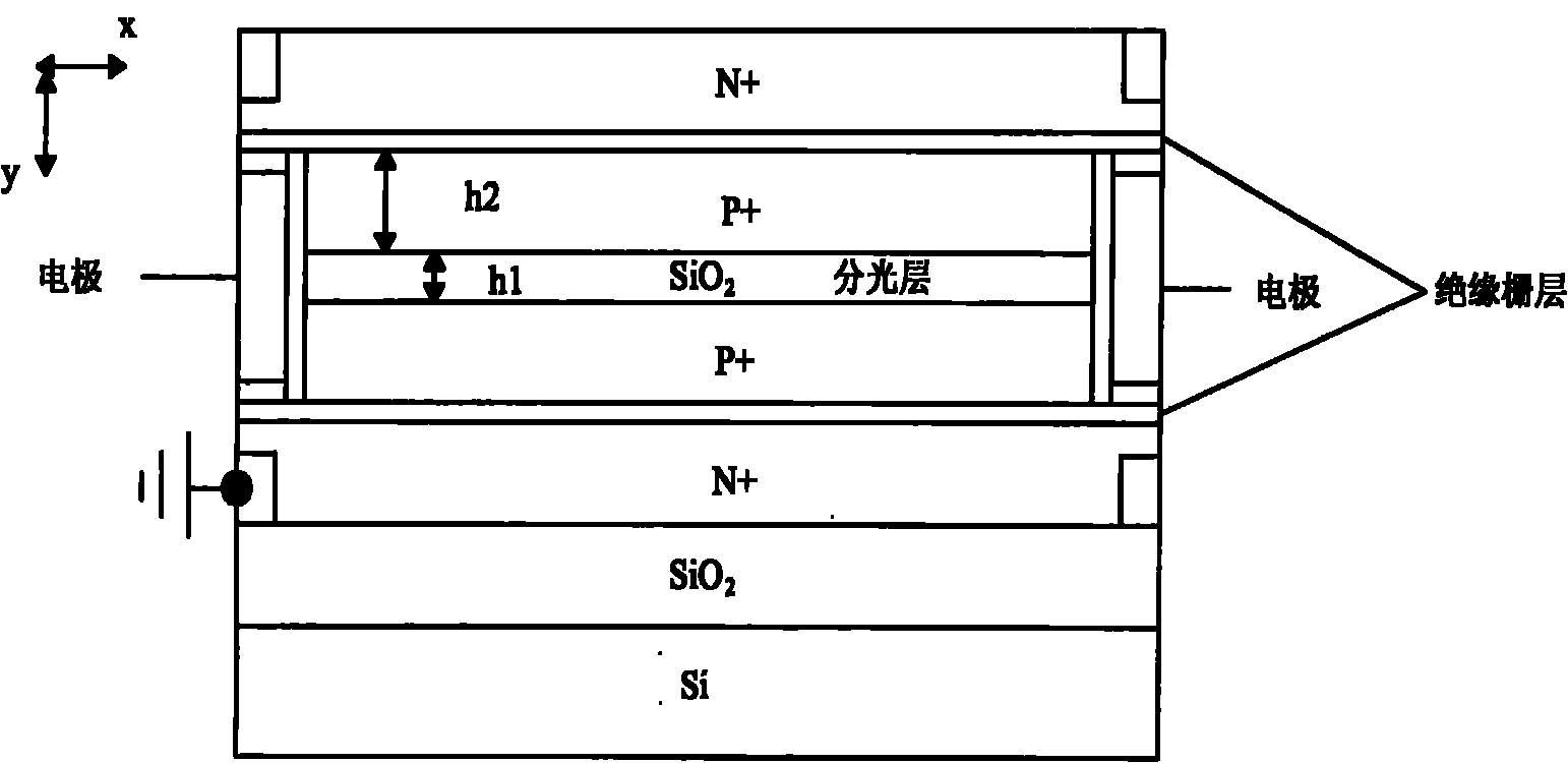
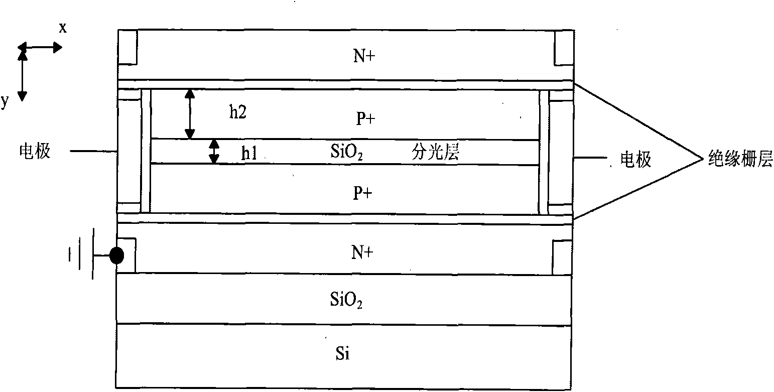
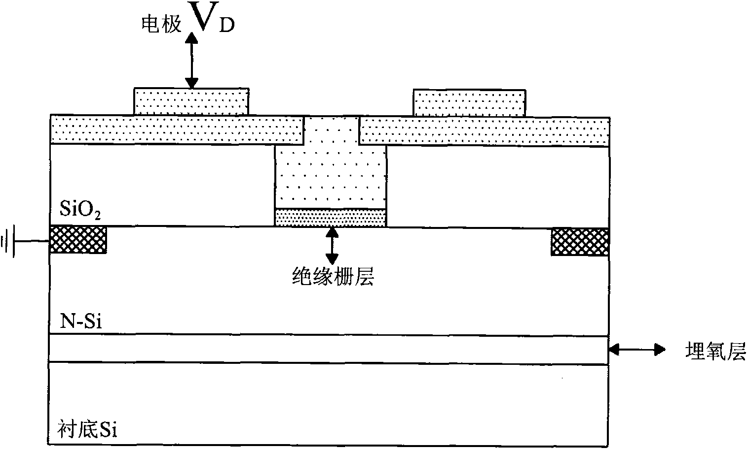
[0019] The silicon-based electro-optic modulator with dual MOS structure proposed by the present invention is described in detail as follows with reference to the drawings and embodiments.

[0020] The silicon-based electro-optic modulator with a dual MOS structure in this embodiment is based on a MOS capacitor structure and uses two insulating gate layers to form a dual MOS structure. This double MOS structure can increase the region where the carrier concentration changes, so that the region where the carrier concentration changes overlaps more with the optical field, thereby obtaining a greater effective refractive index change and shortening the length of the modulator. , reducing the size of the device. The electro-optic modulator with double insulating gate layer structure is characterized by having two insulating gate layers. When a voltage is applied, both insulating gate layers can induce charges, increase the area where the carrier concentration changes, and increas...


PUM

PropertyMeasurementUnit
Thicknessaaaaaaaaaa
Thicknessaaaaaaaaaa

Abstract

The invention relates to a dual-MOS structure silicon-based electro-optical modulator. The structure of the modulator comprises the following parts from top to bottom respectively: a top-layer silicon waveguide layer, a top layer insulated gate layer, a middle layer silicon waveguide layer, a bottom layer insulated gate layer, a bottom layer silicon waveguide layer, a buried oxide SiO2 layer and a Si substrate, wherein the top layer silicon waveguide layer and the bottom layer silicon waveguide layer are N-type doped silicon layers; the middle layer silicon waveguide layer is a P-type doped silicon layer; the middle part of the P-type doped silicon layer is provided with a light splitting layer which is divided into two layers with the same thickness; and the light splitting layer splits an incident beam into two beams of same light propagations. The structure also comprises a grounding electrode arranged on the N-type doped silicon layer and a metal electrode arranged on the P-type doped silicon layer, and the insulated gate layers are made of a SiO2 material. The dual-MOS structure silicon-based electro-optical modulator has quick modulation speed, high efficiency and small device dimension, can adopt different gate materials and different dimensions and can select different doping densities.

Description

technical field [0001] The invention relates to the technical field of silicon-based electro-optic modulators, in particular to a silicon-based electro-optic modulator with a double MOS structure. Background technique [0002] As a traditional material in the field of microelectronics, silicon material has many advantages such as wide source, good mechanical properties, high temperature resistance, low light absorption in the optical communication band, low cost, mature process technology, etc. The first choice for cost OEIC (Optics Electronic Integrated Circuit, optoelectronic integrated circuit). At present, silicon-based high-speed electro-optic modulators with operating wavelengths in the 1.3um and 1.5um optical communication bands are the focus of international research. It is the core device in the (Optical Add-Drop Multiplexer, OADM) system, and it also has great application prospects in chip optical interconnection and optical computing technology. [0003] The sil...

Claims


Application Information

Patent Timeline
IPC IPC(8): G02F1/025
Inventor 周治平毛岸郜定山朱梦霞
Owner PEKING UNIV
Why Eureka
Try Eureka