An nfc antenna

An antenna and conductive coil technology is applied in the field of thimble contact solutions to achieve the effects of reducing costs, shortening product cycles, and having wide applicability

Active Publication Date: 2018-08-03
SHENZHEN SUNLORD ELECTRONICS
View PDF10 Cites 0 Cited by
  • Summary
  • Abstract
  • Description
  • Claims
  • Application Information

AI Technical Summary

Problems solved by technology

[0007] The main purpose of the present invention is to propose an NFC antenna with contacts arranged in a dot matrix to solve the technical problem that the existing NFC antenna needs to customize the design of the contacts according to the specific circuit board

Method used


Image

  • An nfc antenna
  • An nfc antenna
  • An nfc antenna

Examples


Embodiment 1

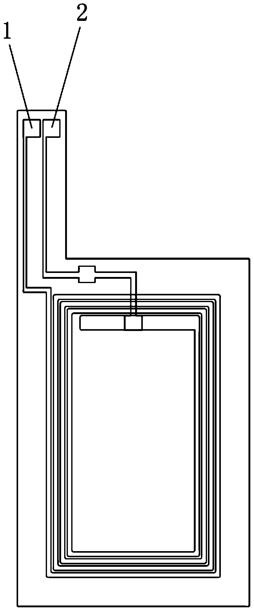
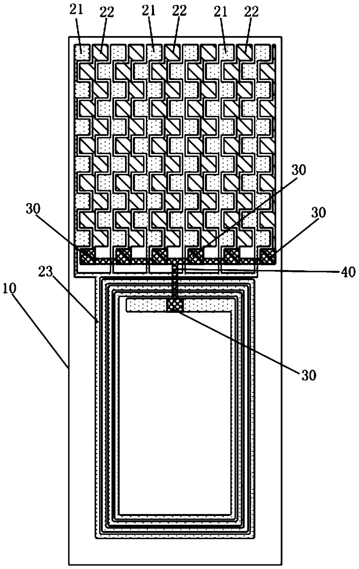
[0027] This specific embodiment provides a kind of figure 2 The NFC antenna shown, in order to show the formation of the antenna loop more clearly, figure 2 The middle and lower surfaces adopt perspective; in the contact array on the upper surface of the substrate 10 , the contacts are divided into two types: the first contact unit 21 and the second contact unit 22 . Such as Figure 4 As shown, the conductive pattern 40 on the lower surface of the substrate can be, for example, T-shaped, and one conductive via 30 a among the plurality of conductive vias 30 is located at the inner ring end 23 b of the conductive coil 23 . Such as image 3 Shown:

[0028] In the first column of contacts, the first, third, fifth, seventh...that is, the contacts in odd rows all belong to the same type of contacts, for example, the first contacts, and the adjacent first contacts in this column pass through wire connection, and is connected to the outer coil end 23a of the conductive coil 23 t...

Embodiment 2

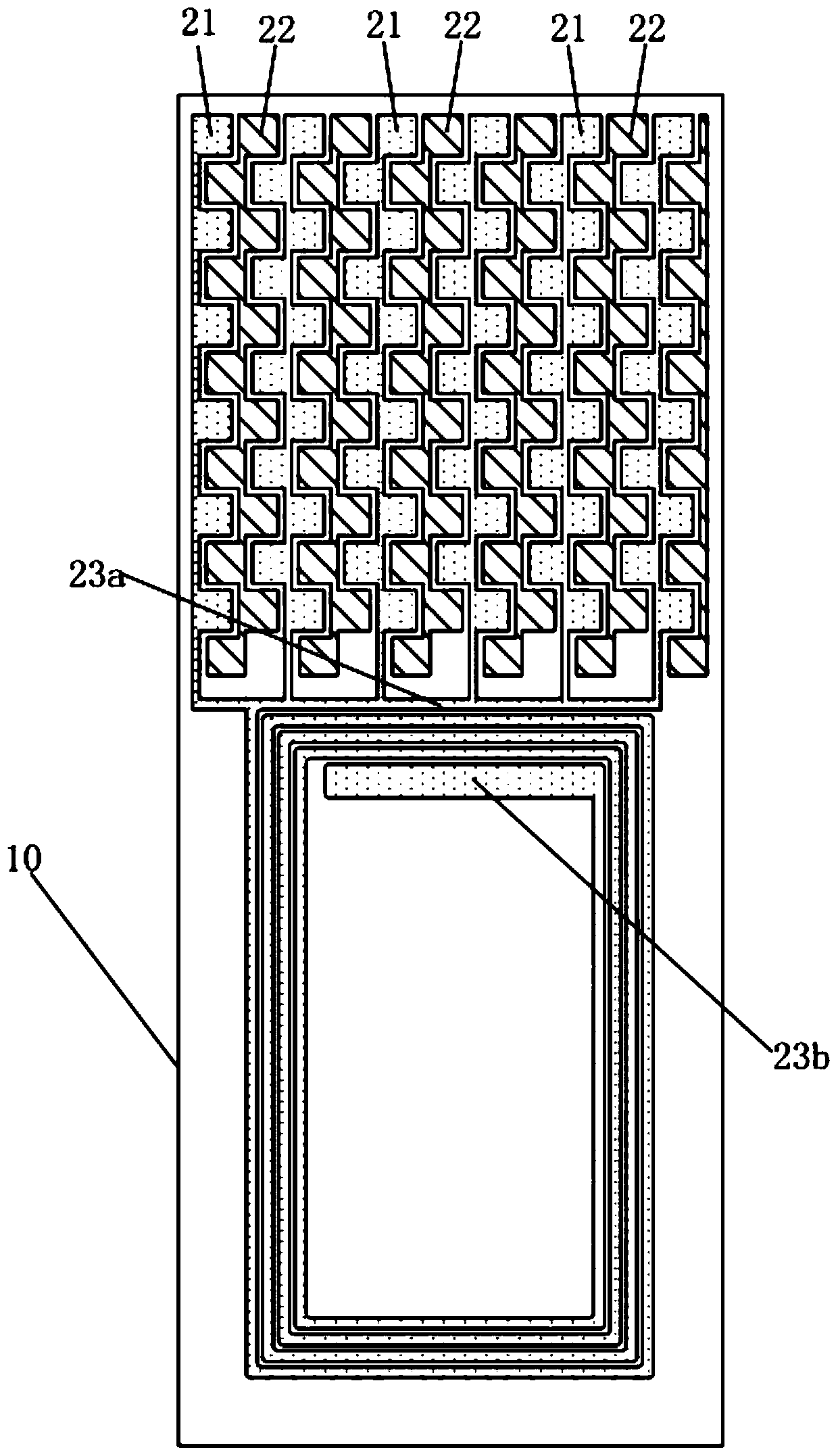
[0037] This embodiment provides a Figures 6 to 8 The NFC antenna shown, such as Figure 6 As shown, the difference between this embodiment and Embodiment 1 is that in the array contacts on the upper surface of the substrate, the connection between the first contacts in the first contact unit 21' is on the upper surface of the substrate, while The connection between the second contacts in the second contact unit 22' is on the lower surface of the substrate.

[0038]The connection mode between the first contacts can be, for example: each first contact is connected to the closest contacts around it, and the connection line between the first contacts runs through the gap between the two second contacts. line, thus forming a Figure 6 Connections are shown, ie, contacts located at the edge of the array are connected to only one or two surrounding contacts, while contacts located inside the array are connected to four surrounding contacts in a four-pointed star connector.

[003...


PUM


Abstract

The invention discloses an NFC antenna, which is connected to a circuit board through a thimble, comprising: a substrate; a first contact unit, a second contact unit and a conductive coil located on the upper surface of the substrate; wherein the first contact unit includes multiple a first contact for connecting to the positive pole of the thimble, the second contact unit includes a plurality of second contacts for connecting to the negative pole of the thimble; a plurality of conductive via holes penetrating the substrate, Connected to each other through the conductive pattern located on the lower surface of the substrate; the first contact is connected to the outer ring of the conductive coil, and the second contact is connected to the inner ring of the conductive coil through the conductive via hole and the conductive pattern The connection; the first contacts and the second contacts are arranged in a dot matrix, and each row includes the first contacts and the second contacts arranged at intervals, and each column includes the first contacts arranged at intervals. contact and the second contact. The array contact design can meet a variety of thimble contacts, without the need for custom-designed antennas.

Description

technical field [0001] The invention relates to an NFC antenna, in particular to an NFC antenna connected to a circuit board through thimble contact, which can be applied to various thimble contact solutions of different specifications. Background technique [0002] At present, there are mainly two ways to connect the NFC (Near Field Communication, near field communication) antenna to the circuit board. One is through a connecting cable, one end of the cable is welded to the contact pad of the NFC antenna, and the other end is welded or crimped to the circuit board. The other way is to contact through the thimble, first fix the thimble on the circuit board, and then press the other end of the thimble to the NFC antenna contact by pressure. [0003] The welding method of connecting wires requires manual assembly, which is complicated in process and high in cost. Moreover, signal interference and EMI problems are likely to occur due to long cables, so it is rarely used in the ...

Claims


Application Information

Patent Timeline
Patent Type & Authority Patents(China)
IPC IPC(8): H01Q1/50H01Q7/00
Inventor 刘宁伍隽
Owner SHENZHEN SUNLORD ELECTRONICS
Why Eureka
Try Eureka