
Simulation model of high voltage device and modeling method for simulation model of high voltage device

A technology of high-voltage devices and simulation models, applied in the fields of electric solid-state devices, semiconductor devices, design optimization/simulation, etc., can solve the problems of time-consuming accuracy, low efficiency, inability to fit high-voltage characteristics well, and achieve high simulation accuracy , the effect of improving the simulation accuracy

Active Publication Date: 2015-11-25
CSMC TECH FAB2 CO LTD
View PDF3 Cites 10 Cited by
  • Summary
  • Abstract
  • Description
  • Claims
  • Application Information

AI Technical Summary

Problems solved by technology

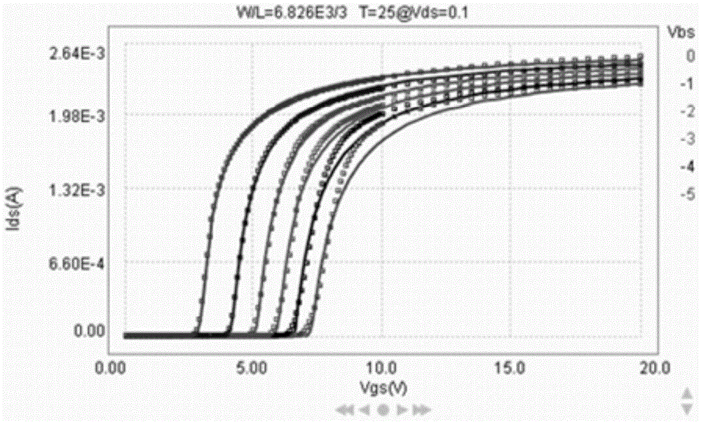
As a result, the most widely used standard models in the industry, BSIM3 and BSIM4, cannot fit this high-voltage characteristic well
Current simulation models for high-voltage devices are costly, inefficient, time-consuming, and inaccurate
Especially for ultra-high voltage devices with a drain-source voltage of more than 700V, the current simulation model is difficult to meet the simulation accuracy requirements

Method used


Image

  • Simulation model of high voltage device and modeling method for simulation model of high voltage device
  • Simulation model of high voltage device and modeling method for simulation model of high voltage device
  • Simulation model of high voltage device and modeling method for simulation model of high voltage device

Examples


Embodiment Construction

[0021] In the following description, numerous specific details are given in order to provide a more thorough understanding of the present invention. It will be apparent, however, to one skilled in the art that the present invention may be practiced without one or more of these details. In other examples, some technical features known in the art are not described in order to avoid confusion with the present invention.

[0022] In order to thoroughly understand the present invention, detailed steps will be presented in the following description to explain the simulation model of the high voltage device and the modeling method of the simulation model of the high voltage device proposed by the present invention. Obviously, the practice of the invention is not limited to specific details familiar to those skilled in the semiconductor arts. Preferred embodiments of the present invention are described in detail below, however, the present invention may have other embodiments besides...


PUM


Abstract

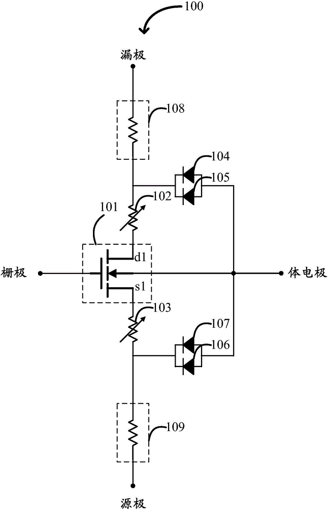
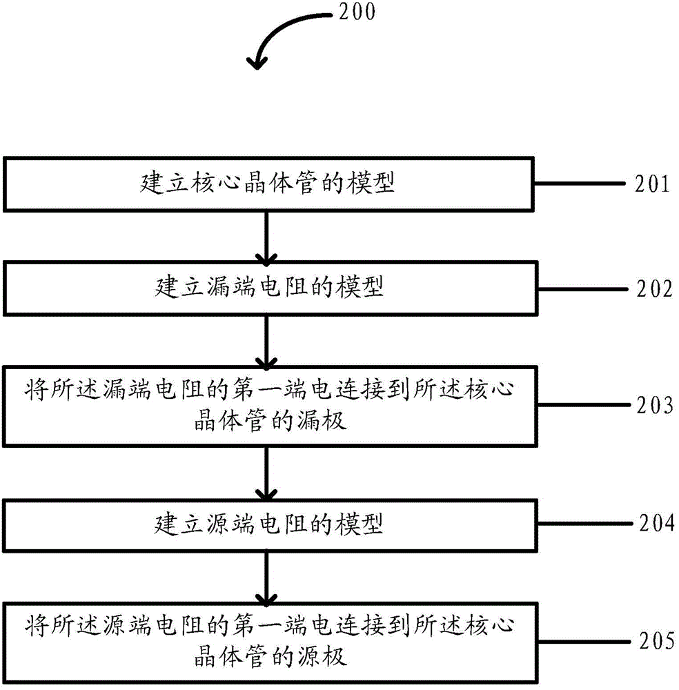
A high-voltage device simulation model and a modeling method therefor. The simulation model comprises: a core transistor (101), a drain end resistor (102) and a source end resistor (103), wherein a first end of the drain end resistor (102) is electrically connected to a drain (d1) of the core transistor (101) and a second end of the drain end resistor (102) serves as the drain of a high voltage device; a first end of the source end resistor (103) is electrically connected to a source (s1) of the core transistor (101) and a second end of the source end resistor (103) serves as the source of the high voltage device. The relations of the resistance value of the drain end resistor (102) are as follows: RD=(RD0 / W)*(1+CRD*VD ERDD+1 / (1+PRWDD*VDERDD))*TFAC_RD, and TFAC_RD=(1+TCRD1*(TEMP-25)+TCRD2*(TEMP-25)*(TEMP-25)).

Description

technical field [0001] The invention relates to the field of integrated circuits, in particular to a simulation model of a high-voltage device and a modeling method of the simulation model of the high-voltage device. Background technique [0002] In recent years, high-voltage devices are more and more widely used in integrated circuit products, for example, they can be used in circuits such as power management chips. With the wide application of high-voltage devices, the accuracy requirements of high-voltage device simulation models in integrated circuit design are also getting higher and higher. The special structure of high-voltage devices determines that these devices have more parasitic effects, such as the typical quasi-saturation effect. The quasi-saturation effect means that when the gate voltage increases, compared with ordinary MOSFET transistors, the saturation current increase speed of high-voltage transistor devices is significantly reduced, that is, the control...

Claims


Application Information

Patent Timeline
Patent Type & Authority Applications(China)
IPC IPC(8): G06F17/50
CPCG06F17/50G06F2119/06G06F30/367G06F30/00Y02E60/00Y04S40/20G06F30/20H01L27/0207
Inventor 胡一峰何小东刘新新
Owner CSMC TECH FAB2 CO LTD
Learn More