Chip screening method and apparatus

A screening method and chip technology, applied in the field of communication, can solve problems such as high cost, low reliability, and high subjectivity, and achieve the effect of reducing screening cost and high reliability

Active Publication Date: 2015-11-25
HUAWEI TECH CO LTD
View PDF5 Cites 7 Cited by
  • Summary
  • Abstract
  • Description
  • Claims
  • Application Information

AI Technical Summary

Problems solved by technology

However, manual screening not only takes up a lot of manpower, but also has the problem of high cost, and manual designation has inconsistent standards between different personnel and different batches, which is highly subjective, may have the problem of over-killing or under-killing, and has low reliability.

Method used


Image

  • Chip screening method and apparatus
  • Chip screening method and apparatus
  • Chip screening method and apparatus

Examples


Embodiment Construction

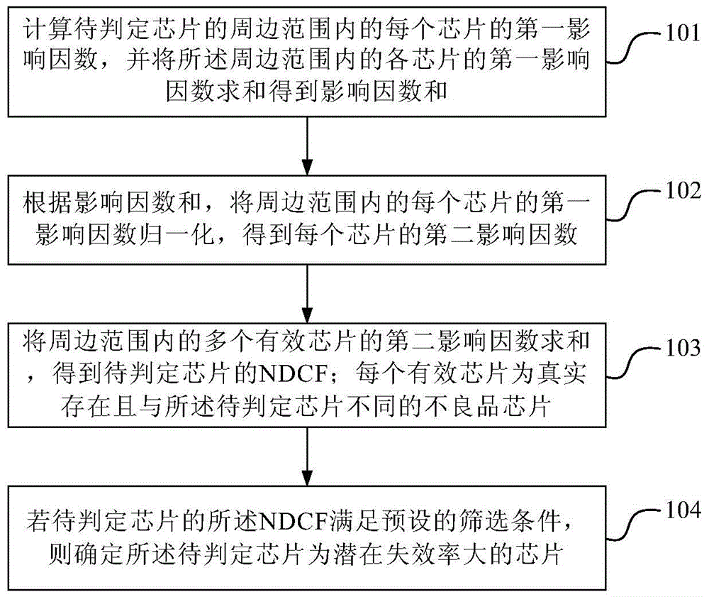
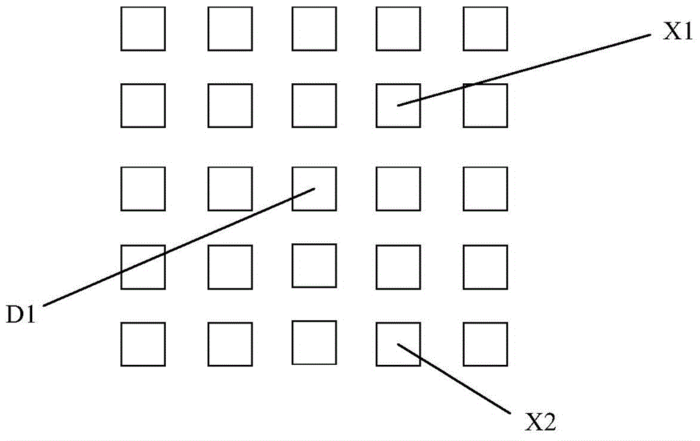
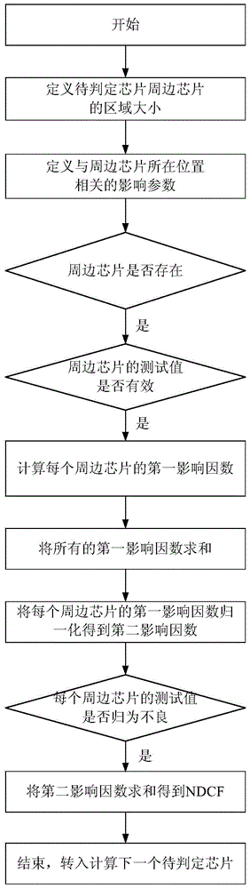
[0037] The chip screening method described in the embodiment of the present invention is a method of data statistics and probability statistics, which is based on the WaferMap (wafer mapping) data reflecting the situation of good chips obtained from the wafer test (WaferCP test). The peripheral range chips of the good product (PassDie) obtained in the pass die are counted to evaluate the possibility of potential failure of the good product chip. It should be noted that the term "chip" mentioned in the following example description, if it is applied to the description of wafer (Wafer), should actually be called wafer "Die". For the sake of uniformity, the full text is written as " chip". Therefore, the chip may be various types of semiconductor devices produced by semiconductor processing techniques such as wafers or wafers. In wafer testing, multiple chips are placed on a plane or platform with a certain distance from each other, and the distance between each chip can be equa...


PUM


Abstract

The present invention provides a chip screening method and apparatus. The method comprises: calculating a first influence factor of each chip within a peripheral range of a to-be-determined chip, and summing the first influence factors of the chips within the peripheral range to obtain a sum of the influence factors; normalizing the first influence factor of each chip within the peripheral range based on the sum of the influence factors to obtain a second influence factor; summing the second influence factors of effective chips within the peripheral range to obtain a correlation factor NDCF of the peripheral chips of the to-be-determined chip; and if the NDCF of the to-be-determined chip meets predefined screening criteria, determining that the to-be-determined chip is a chip with a large potential failure rate. The present invention reduces chip screening costs.

Description

technical field [0001] The embodiments of the present invention relate to communication technologies, and in particular to a chip screening method and device. Background technique [0002] The Factory Defective Parts Per Million (FDPPM) requirement for carrier-grade products is usually high. How to improve the quality of shipments and reduce the FDPPM of chips is the primary issue for manufacturers to improve profitability and customer satisfaction. One of the main reasons for the high FDPPM is the high early failure rate (Early Failure Rate, referred to as: EFR) of the chip. Screening out chips that may cause potential failure risks in the mass production test of the chip is a method to reduce the EFR. For example, a chip that is judged as a FailDie in the wafer test, although the surrounding PassDie can meet the wafer test specifications, the probability of early failure of these passDie chips is higher than that of passDie in other locations. , that is, the potential ris...

Claims


Application Information

Patent Timeline
Patent Type & Authority Applications(China)
IPC IPC(8): G06F19/00
Inventor 崔禾捷张国强钟进国
Owner HUAWEI TECH CO LTD
Why Eureka
Try Eureka