Pixel circuit and driving method thereof as well as display apparatus

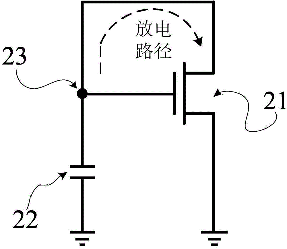
A pixel circuit and capacitor technology, applied in the field of display devices, can solve the problems of incomplete discharge of the storage capacitor 22, difficulty in accurately determining the programming time, etc., and achieve the effect of compensating for threshold voltage shift and taking into account speed and accuracy.

Active Publication Date: 2015-11-25
PEKING UNIV SHENZHEN GRADUATE SCHOOL
View PDF8 Cites 21 Cited by
  • Summary
  • Abstract
  • Description
  • Claims
  • Application Information

AI Technical Summary

Problems solved by technology

On the one hand, if the programming time is too short, the discharge of the storage capacitor 22 will not be complete, so that the extracted threshold voltage (the voltage of node 23) is higher than the actual value; on the other hand, if the programming time is too long, when the drive tube 21 After the threshold extraction is completed, the driving tube 21 starts to enter the sub-threshold region, and the storage capacitor 22 will continue to discharge through the driving tube 21, resulting in the extracted threshold voltage being lower than the real threshold voltage value
However, in the actual application process, when the threshold voltage of the drive tube 21 and the threshold voltage of the light emitting device OLED14 degenerate, it will be difficult to accurately determine the programming time

Method used


Image

  • Pixel circuit and driving method thereof as well as display apparatus
  • Pixel circuit and driving method thereof as well as display apparatus
  • Pixel circuit and driving method thereof as well as display apparatus

Examples


Embodiment 1

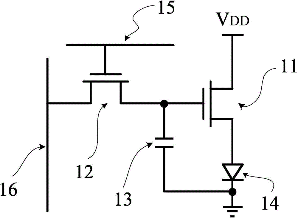
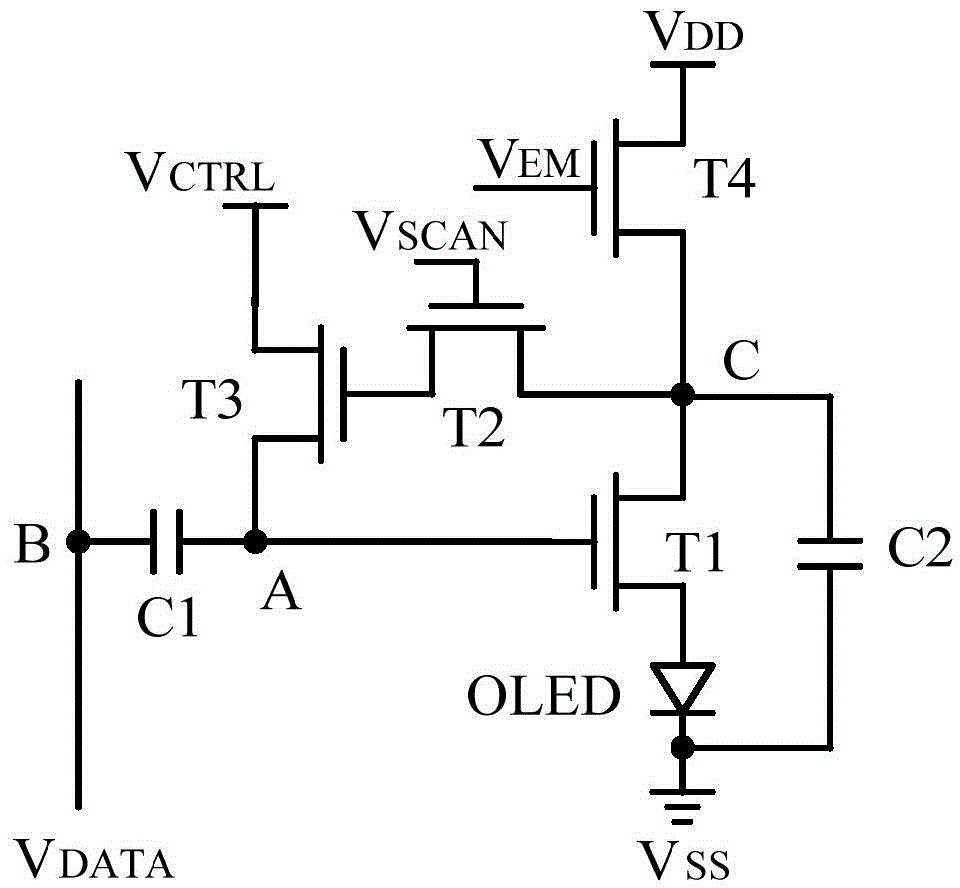
[0044] Please refer to image 3 , image 3 Shown is the structure of an embodiment of the pixel circuit of the present application, including: a first capacitor C1, a second capacitor C2, a second transistor T2, a third transistor T3, and a capacitor for coupling between the first common electrode VDD and the second common electrode Lighting branch between VSS. The light emitting branch circuit includes a first transistor T1, a fourth transistor T4 and a light emitting element OLED connected in series.

[0045] Wherein, the first pole of the first transistor T1 is coupled to the second pole of the fourth transistor T4, and the coupling node is the third node C; the control pole of the fourth transistor T4 is used to input the second scanning control signal V EM , the fourth transistor T4 responds to the second scan control signal V EM Switch the on and off state of the light-emitting branch.

[0046] The first end of the first capacitor C1 is the second node B for coupling...

Embodiment 2

[0070] The circuit provided by Embodiment 1 adopts a concentrated light emitting method. For a display device, it needs to wait for the data signals of all rows of pixel arrays to be written before entering the light emitting stage. It is advisable to set the number of rows of the pixel array as n(n is a positive integer), when the kth (k≤n, positive integer) row pixel programming stage is completed, it is necessary to wait for the k+1 to nth row pixel programming to be completed, and the pixel array enters the light emitting stage at the same time. With the concentrated light emitting method, the light emitting time of the pixel array is short and the current required is large, which may accelerate the degradation of the light emitting element OLED.

[0071] To this end, this embodiment discloses a pixel circuit of non-concentrated light emitting mode, please refer to Figure 6 and Figure 7 , is the structure of the pixel circuit in this embodiment. The difference from the ...

Embodiment 3

[0091] Please refer to Figure 9 and Figure 10 , which is the structural diagram of the pixel circuit disclosed in this embodiment. The difference from the above-mentioned embodiments is that the pixel circuit disclosed in this embodiment further includes a fifth transistor T5, and the first pole and the second pole of the fifth transistor T5 are connected in parallel to the light-emitting element Both ends of the OLED, the gate is used to input the first scan control signal V SCAN .

[0092] When the light-emitting element OLED is in a non-light-emitting state, the fifth transistor T5 is turned on, and when the light-emitting element OLED is in a light-emitting state, the fifth transistor T5 is turned off. Specifically: in the initialization stage and the programming stage, the fifth transistor T5 responds to the first scanning control signal V SCAN The high level is turned on; in the light emitting stage, the fifth transistor T5 responds to the first scanning control sig...


PUM


Abstract

A pixel circuit, a drive method based on the pixel circuit, and a display device. The pixel circuit comprises: a first capacitor (C1), a second capacitor (C2), a second transistor (T2), a third transistor (T3) and a light-emitting branch for being coupled between a first common electrode (VDD) and a second common electrode (VSS); wherein the light-emitting branch comprises a first transistor (T1), a fourth transistor (T4) and a light-emitting element (OLED) which are connected in series; a first electrode of the first transistor (T1) is coupled to a second electrode of the fourth transistor (T4), and a coupling node is a third node (C); and a control electrode of the fourth transistor (T4) is used for inputting a second scanning control signal (V EM), and the fourth transistor (T4) switches the ON/OFF state of the light-emitting branch in response to the second scanning control signal (V EM). At the programming stage, a threshold voltage of the first transistor (T1) is input to a first node (A) through the third transistor (T3) and is stored; and at the light-emitting stage, a light-emitting current for driving the light-emitting element (OLED) is generated according to information about a voltage difference across two ends of the first capacitor (C1). The pixel circuit is used for compensating for the threshold voltage shift of the first transistor (T1) and the light-emitting element (OLED).

Description

technical field [0001] The present application relates to the field of display devices, in particular to a pixel circuit, a driving method thereof, and a display device. Background technique [0002] Organic Light-Emitting Diode (OLED) displays have been extensively studied in recent years due to their advantages of high brightness, high luminous efficiency, wide viewing angle and low power consumption, and have been rapidly applied to a new generation of displays. The OLED display can be driven in two ways: passive matrix driving (PassiveMatrixOLED, PMOLED) and active matrix driving (ActiveMatrixOLED, AMOLED). Although the cost of passive matrix driving is low, it cannot realize high-resolution display due to crosstalk phenomenon, and the passive matrix driving current is large, which reduces the service life of OLED. In contrast, the active matrix driving method sets a different number of transistors on each pixel as a current source, which avoids crosstalk, requires less...

Claims


Application Information

Patent Timeline
Patent Type & Authority Applications(China)
IPC IPC(8): G09G3/32
CPCG09G3/3233G09G3/3291G09G2300/0819G09G2300/0852G09G2300/0861G09G2310/08G09G2320/043G09G2300/043G09G2300/0439
Inventor 张盛东王翠翠冷传利王龙彦
Owner PEKING UNIV SHENZHEN GRADUATE SCHOOL
Why Eureka
Try Eureka