Chip electronic component and board for mounting thereof

An electronic component and chip technology, which is applied in the direction of printed circuits, electrical components, and printed electrical components connected with non-printed electrical components, and can solve problems such as the limitation of inductor characteristics.

Active Publication Date: 2015-11-25
SAMSUNG ELECTRO MECHANICS CO LTD
View PDF6 Cites 6 Cited by
  • Summary
  • Abstract
  • Description
  • Claims
  • Application Information

AI Technical Summary

Problems solved by technology

[0011] However, previous coil structures fabricated by substrate plating processes did not include the improved coil structure features desc

Method used


Image

  • Chip electronic component and board for mounting thereof
  • Chip electronic component and board for mounting thereof
  • Chip electronic component and board for mounting thereof

Examples


Embodiment Construction

[0029] Embodiments in the present disclosure will now be described in detail with reference to the accompanying drawings.

[0030] Embodiments may, however, be embodied in many different forms and should not be construed as limited to the embodiments set forth herein. Rather, these embodiments are provided so that this disclosure will be thorough and complete, and will fully convey the scope of the inventive concept to those skilled in the art. In the drawings, the shapes and sizes of elements may be exaggerated for clarity.

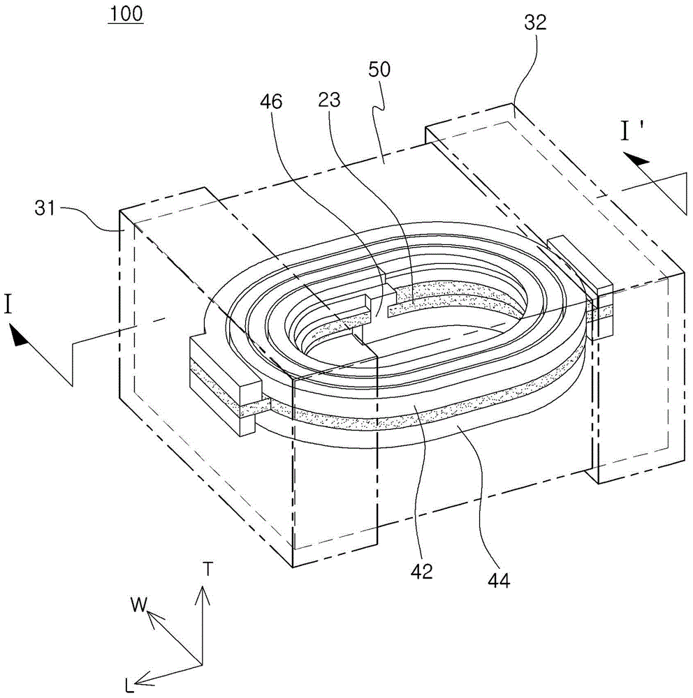
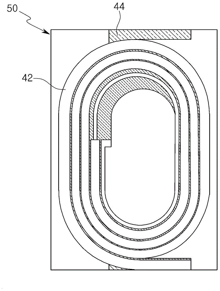
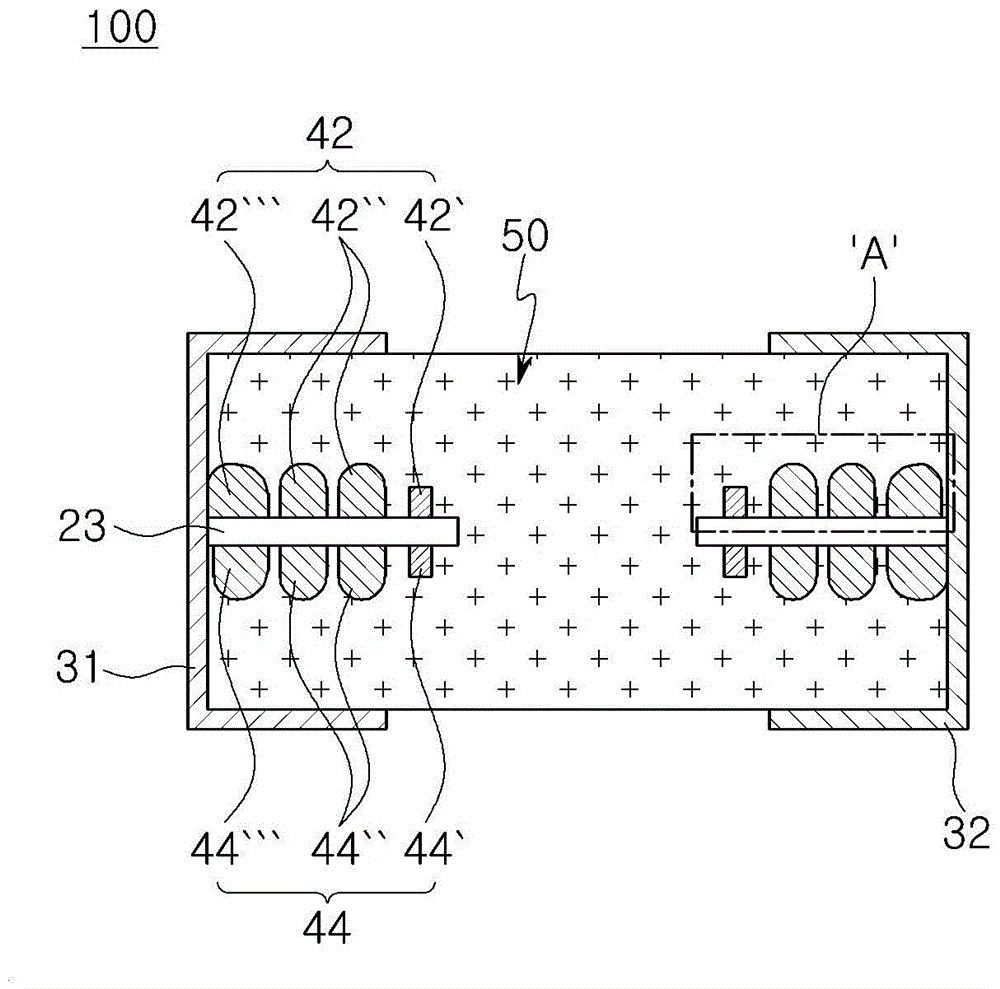
[0031] chip electronic components

[0032] A chip type electronic component according to an exemplary embodiment of the present disclosure, that is, a thin film type inductor will be described. However, the present disclosure is not limited thereto.

[0033] figure 1 is a schematic perspective view showing a chip-type electronic assembly according to an exemplary embodiment in the present disclosure, in figure 1 The internal coil pattern of the ch...


PUM


Abstract

A chip electronic component may include a magnetic material body including an insulating substrate and coil conductor patterns formed on at least one surface of the insulating substrate, and external electrodes disposed on both end portions of the magnetic material body so as to be connected to end portions of the coil conductor patterns, respectively. In a cross section of the magnetic material body in a length direction, a thickness of an innermost loop/section of the coil conductor patterns may be smaller than a thickness of the remaining loops/sections of the coil conductor pattern.

Description

[0001] This application claims the benefit of Korean Patent Application No. 10-2014-0060769 filed with the Korean Intellectual Property Office on May 21, 2014, the disclosure of which is hereby incorporated by reference. technical field [0002] The present disclosure relates to a chip type electronic component and a board for mounting the chip type electronic component. Background technique [0003] Inductors, which are chip electronic components, may be representative passive elements constituting electronic circuits, and may be used for noise removal together with resistors and capacitors, for example. Such inductors can be combined with such capacitors using electromagnetic properties to construct circuits such as resonant circuits, filter circuits, etc. For example, such inductors can be used to amplify signals in specific frequency bands. [0004] Recently, since miniaturization and thinning of various information technology (IT) devices such as communication devices, ...

Claims


Application Information

Patent Timeline
IPC IPC(8): H01F17/00H01F27/28H05K1/18
CPCH05K1/165H05K3/241H05K2201/0347H05K2201/086H05K2201/09727H05K2201/09736H05K2201/098H05K2201/10636H05K2203/1476H01F17/0013H01F2017/0066H01F2017/0073H01F27/292H05K2201/1003Y02P70/50H01F27/24H01F27/2804H01F2027/2809H05K1/111H05K1/181
Inventor 李东焕尹灿车慧娫韩镇宇
Owner SAMSUNG ELECTRO MECHANICS CO LTD
Why Eureka
Try Eureka