High-voltage power device and forming method thereof

A high-voltage power device and device technology, which is applied in the direction of semiconductor devices, semiconductor/solid-state device manufacturing, electrical components, etc., can solve problems such as unstable withstand voltage, reduced current capacity of devices, and high concentration

Active Publication Date: 2015-11-25
HANGZHOU SILAN MICROELECTRONICS
View PDF6 Cites 7 Cited by
  • Summary
  • Abstract
  • Description
  • Claims
  • Application Information

AI Technical Summary

Problems solved by technology

[0007] use figure 2 Although the compensation matching degree of the device decreases and a small part of the withstand voltage is sacrificed, the tolerance of the charge compensation is improved, that is, when the impurity concentration in the compensation region does not reach the best matching degree, the first doped region 206 and the The impurity concentration of the second doped region 210 can obtain a higher withstand voltage within a certain deviation range, which solves the situation of unstable withstand voltage
[0008] As mentioned above, although the methods proposed in US patent documents US6630698 and US6894329 have solved the problem of withstand voltage stability, due to the monotonous linear increase in concentration, in the area near the second electrode, the concentration of the second doped region is higher than that of first doped region
When the device is turned on, the current channel formed by the first doped region is narrowed in this region by the increase of the impurity concentration of the second doped region, that is, the so-called JFET resistance increases, resulting in an increase in the on-resistance of the device, The current capability of the device degrades

Method used


Image

  • High-voltage power device and forming method thereof
  • High-voltage power device and forming method thereof
  • High-voltage power device and forming method thereof

Examples


no. 1 example

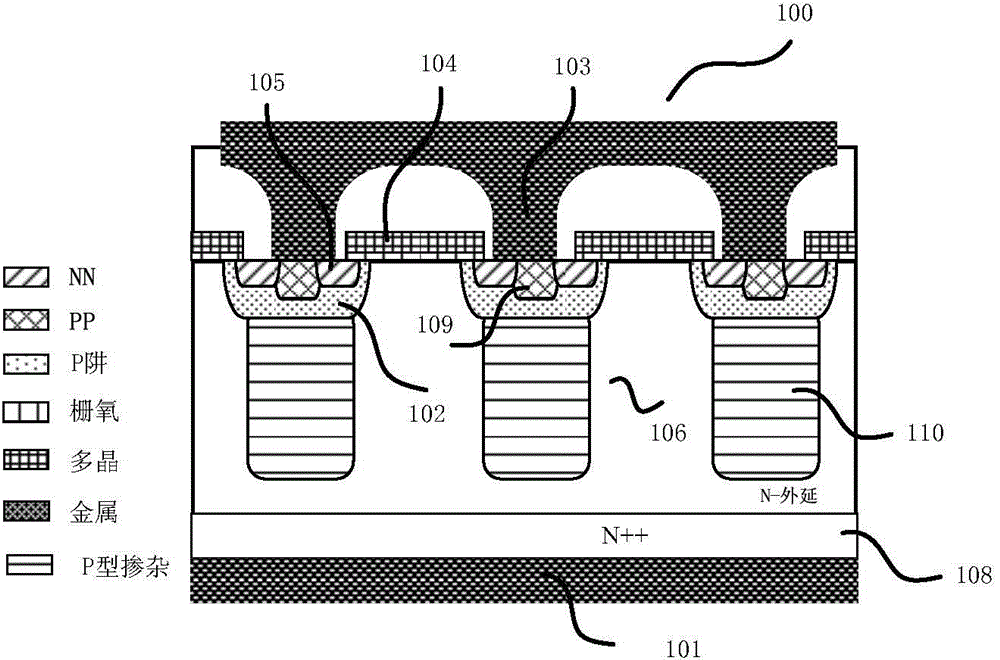
[0129] refer to image 3 , image 3 The shown high-voltage power device 300 is a high-voltage MOS device, which mainly includes: an N-type first doped region 306 located on an N-type doped substrate 308; a first electrode 301 connected to the first doped region via the substrate 308 The impurity region 306 is in electrical contact; a plurality of P-type well regions 302 are arranged laterally in the upper surface of the first doped region 306; the P-type second doped region 310 has one end connected to the well region 302 and the other end Extend vertically into the first doped region 306; the N-type device doped region 305 and the P-type device doped region 309 are formed in the well region 302, and the second doped region 310 is connected to the P-type doped region through the well region 302. The device doping region 309 is in electrical contact; the gate 304 is formed on the upper surface of the first doping region 306; the second electrode 303 is in contact with the N-ty...

no. 2 example

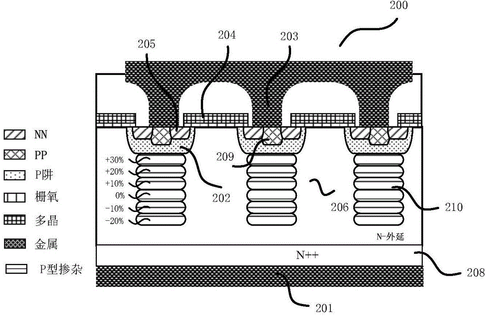
[0136] refer to Figure 4 , Figure 4 The shown high-voltage power device 400 is a high-voltage MOS device, and its structure is the same as image 3 Basically the same, including: an N-type first doped region 406 located on an N-type doped substrate 408; a first electrode 401 electrically contacting the first doped region 406 via the substrate 408; a plurality of P-type The well region 402 is horizontally arranged in the upper surface of the first doped region 406; the P-type second doped region 410 has one end connected to the well region 402, and the other end extends vertically into the first doped region 406; The N-type device doping region 405 and the P-type device doping region 409 are formed in the well region 402, and the second doping region 410 is in electrical contact with the P-type device doping region 409 via the well region 402; the gate 404 is formed on the upper surface of the first doped region 406 ; the second electrode 403 is in electrical contact with t...

no. 3 example

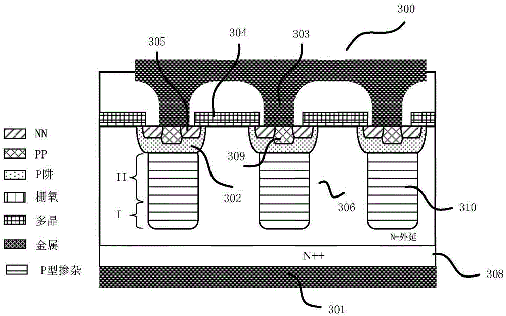
[0154] refer to Figure 12 , Figure 12 The shown high-voltage power device 800 is a high-voltage MOS device, and its structure is the same as image 3 Basically the same, including: an N-type first doped region 806 located on an N-type doped substrate 808; a first electrode 801 electrically contacting the lower surface of the first doped region 806 via the substrate 808; a plurality of The P-type well region 802 is horizontally arranged in the upper surface of the first doped region 806; the P-type second doped region 810 is connected to the well region 802 at one end and extends vertically to the first doped region at the other end. 806; the N-type device doping region 805 and the P-type device doping region 809 are formed in the well region 802, and the second doping region 810 is in electrical contact with the P-type device doping region 809 via the well region 802 The gate 804 is formed on the upper surface of the first doped region 806 ; the second electrode 803 is in ...


PUM


Abstract

The invention provides a high-voltage power device and a forming method thereof. The device comprises a first doped area having a first doped type; one or a plurality of device doped areas arranged in the upper surface of the first doped area, wherein the device doped area has a second doped type opposite to the first doped type; and one or a plurality of second doped areas of the second doped type, wherein one end of the second doped area is in electric contact with a corresponding device doped area, the other end of the second doped area longitudinally extends to the first doped area, and in the transverse direction, the second doped areas and the first doped areas are alternatively distributed. The impurity concentration of each second doped area changes in a non-linear manner with the change of the longitudinal depth, and the total impurity concentration of the second doped areas is lower than the total impurity concentration of the first doped areas. According to the invention, the withstand voltage of the device is stabilized, and the conduction resistance of the device is reduced.

Description

technical field [0001] The invention relates to a high-voltage power device, in particular to a charge-compensated high-voltage power device and a forming method thereof. Background technique [0002] refer to figure 1 , figure 1 A high voltage MOS device structure in the prior art is shown. The high-voltage MOS device 100 includes: a first doped region 106 of the MOS device, the first doped region 106 is an N-type epitaxial region, and the first doped region 106 is drawn out from the first electrode 101 via an N-type doped substrate 108 , forming the drain of the MOS device; the P-type well region 102 of the MOS device; the N-type doped region 105 of the MOS device, forming a source region; the P-type doping region 109 of the MOS device, forming a substrate contact region, and a P-type well The region 102 and the P-type doped region 109 are short-circuited by the second electrode 103 to form the source of the MOS device; the gate 104 of the MOS device; the second doped r...

Claims


Application Information

Patent Timeline
Patent Type & Authority Applications(China)
IPC IPC(8): H01L29/78H01L29/861H01L29/06H01L29/36H01L21/336H01L21/329
Inventor 张邵华曹俊赵金波李敏
Owner HANGZHOU SILAN MICROELECTRONICS
Why Eureka
Try Eureka