Storage unit of flash memory and method for forming same

A technology of storage unit and flash memory, which is applied in the direction of electrical components, electric solid-state devices, circuits, etc., can solve the problems of little performance improvement of flash memory, low data storage time, and weak carrier mobility, etc. Effects of carrier mobility, increased overlap area, and improved programming and reading efficiency

Active Publication Date: 2016-09-14
SHANGHAI HUAHONG GRACE SEMICON MFG CORP
View PDF8 Cites 0 Cited by
  • Summary
  • Abstract
  • Description
  • Claims
  • Application Information

AI Technical Summary

Problems solved by technology

[0005] The prior art flash memory covered with a stress layer does not improve the mobility of carriers strongly, and the data storage time is relatively low, resulting in little improvement in the performance of flash memory

Method used


Image

  • Storage unit of flash memory and method for forming same
  • Storage unit of flash memory and method for forming same
  • Storage unit of flash memory and method for forming same

Examples


Embodiment Construction

[0059] As mentioned in the background art, the flash memory covered with the stress layer in the prior art does not improve the mobility of carriers strongly, and the data storage time is relatively low, resulting in little improvement in the performance of the flash memory.

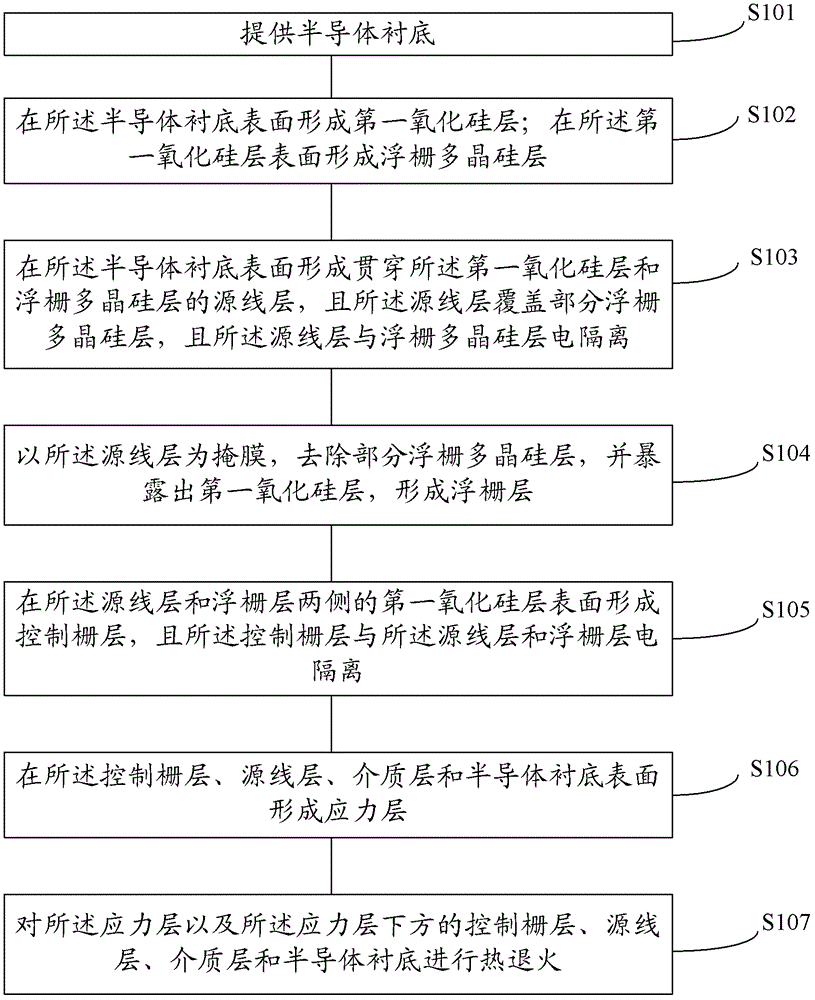
[0060] The inventor of the present invention has carried out research, has proposed a kind of storage unit of flash memory, comprises:

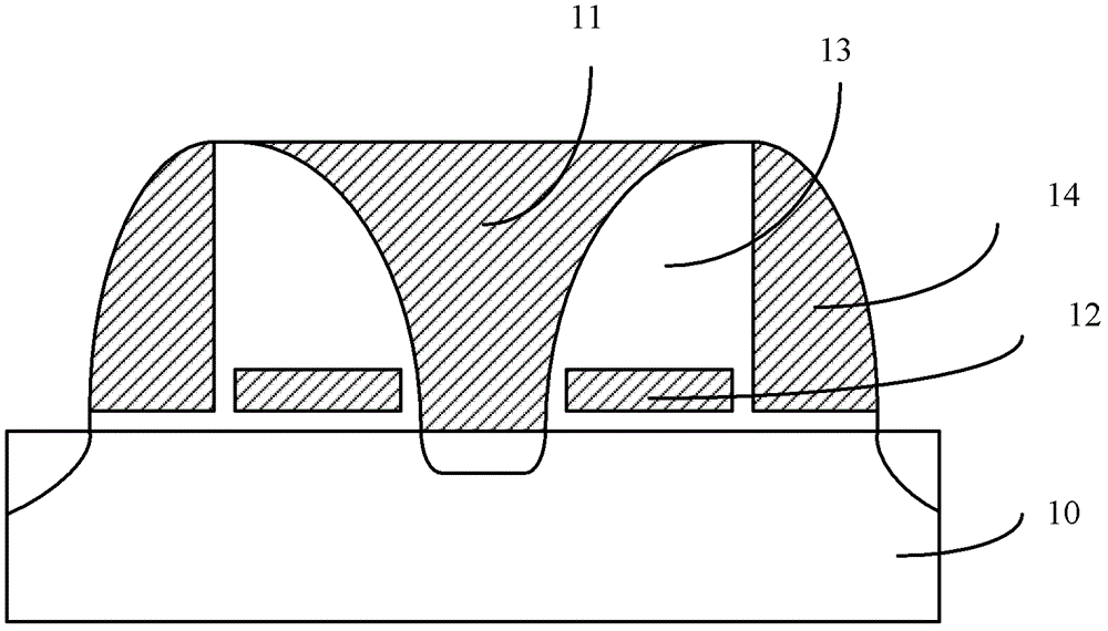
[0061] A semiconductor substrate; an insulating layer located on the surface of the semiconductor substrate; a floating gate layer located on the surface of the insulating layer; a source line layer located on the surface of the semiconductor substrate and passing through the floating gate layer and the insulating layer, and the source The line layer covers the floating gate layer, and the source line layer is electrically isolated from the floating gate layer; the control gate layer located on both sides of the floating gate layer and the source line layer, and the surf...


PUM


Abstract

A storage unit of flash memory and a method for forming the same, wherein the storage unit of flash memory comprises: a semiconductor substrate; an insulating layer located on the surface of the semiconductor substrate; a floating gate layer located on the surface of the insulating layer; The bottom surface and the source line layer that runs through the floating gate layer and the insulating layer, and the source line layer covers the floating gate layer, and the source line layer is electrically isolated from the floating gate layer; Both sides of the line layer, and the control gate layer on the surface of the insulating layer, and the control gate layer is electrically isolated from the source line layer and the floating gate layer; the stress layer located on the control gate layer, the source line layer and the surface of the semiconductor substrate. The storage unit of the flash memory uses the stress effect to improve the programming efficiency and read efficiency of data, improve the retention and durability of data, and further reduce the size of the storage unit of the flash memory.

Description

technical field [0001] The invention relates to the field of semiconductor manufacturing, in particular to a storage unit of a flash memory and a forming method thereof. Background technique [0002] In the current semiconductor industry, integrated circuit products can be mainly divided into three types: analog circuits, digital circuits and digital / analog hybrid circuits, among which storage devices are an important type of digital circuits. In recent years, among storage devices, flash memory (flash memory) has developed particularly rapidly. The main feature of flash memory is that it can keep stored information for a long time without power on; and it has the advantages of high integration, fast access speed, easy erasing and rewriting, etc., so it has been widely used in many fields such as microcomputer and automatic control. a wide range of applications. [0003] In the prior art, please refer to the storage unit of the flash memory figure 1 ,include: [0004] A ...

Claims


Application Information

Patent Timeline
Patent Type & Authority Patents(China)
IPC IPC(8): H01L27/115H01L21/8247
Inventor 于涛胡勇李冰寒
Owner SHANGHAI HUAHONG GRACE SEMICON MFG CORP
Why Eureka
Try Eureka