Display panel and display device

A display panel and display device technology, which is applied to semiconductor devices, electrical components, circuits, etc., can solve the problems of high impedance of signal wires, affecting display, heating of lines, etc., and achieve the effect of increasing current channels, improving yield rate, and preventing heat generation

Active Publication Date: 2022-05-27
WUHAN CHINA STAR OPTOELECTRONICS SEMICON DISPLAY TECH CO LTD
View PDF6 Cites 0 Cited by
  • Summary
  • Abstract
  • Description
  • Claims
  • Application Information

AI Technical Summary

Problems solved by technology

[0005] The present invention provides a display panel and a display device. Aiming at the prior art, during the function test process, due to the excessive impedance of the signal wire in the bending sub-area, the circuit is seriously heated, which causes the circuit to fuse or burn the nearby film layer, and then Technical Issues Affecting Display

Method used


Image

  • Display panel and display device
  • Display panel and display device
  • Display panel and display device

Examples


Embodiment 1

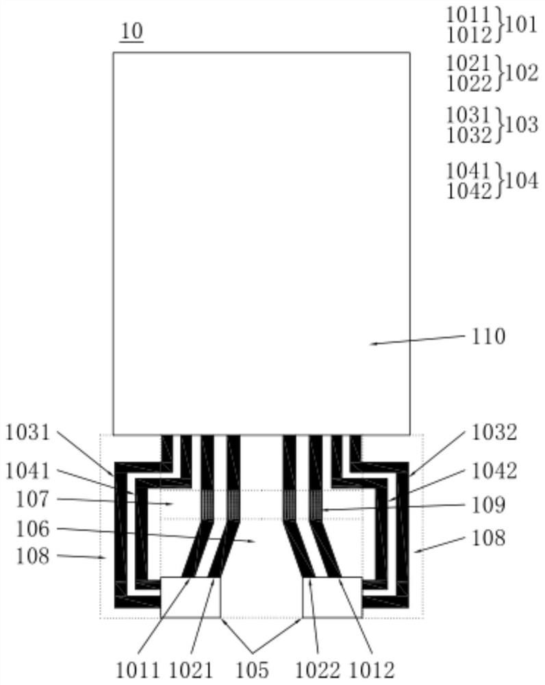
[0069] Please refer to figure 1 As shown, the display panel 10 includes a display area 110 and a non-display area surrounding the display area, the non-display area includes a terminal area 106 disposed on one side of the display area 110, and a terminal area 106 disposed in the terminal area Resection area 108 on both sides of 106 .

[0070] The terminal area 106 is provided with signal wires 101, 102, and the signal wires 101, 102 connect the TFT layer in the display area 110 with the functional circuit in the terminal area 106, which mainly includes the first A VDD trace 1011 , a second VDD trace 1012 , a first VSS trace 1021 and a second VSS trace 1022 .

[0071] The display panel 10 further includes auxiliary wires 103 and 104, and the auxiliary wires 103 and 104 are arranged in the cutout area 108, extend into the terminal area 106, and are connected in parallel with the signal wires 101 and 102. It mainly includes a first VDD auxiliary line 1031 corresponding to the f...

Embodiment 2

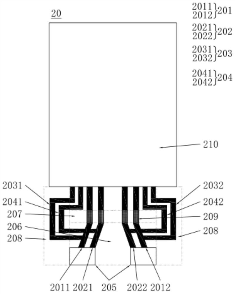
[0077] Please refer to figure 2 As shown, the display panel 20 includes a display area 210 and a non-display area surrounding the display area 210, the non-display area includes a terminal area 206 disposed on one side of the display area 210, and a terminal area 206 disposed on the terminal Cutout regions 208 on either side of region 206 .

[0078] The terminal area 206 is provided with signal wires 201 and 202, and the signal wires 201 and 202 connect the TFT layer in the display area 210 with the functional circuits in the terminal area 206, which mainly include the first A VDD trace 2011 , a second VDD trace 2012 , a first VSS trace 2021 and a second VSS trace 2022 .

[0079] The display panel 20 further includes auxiliary wires 203, 204, and the auxiliary wires 203, 204 are disposed in the cutout area 208, extend into the terminal area 206, and are connected in parallel with the signal wires 201, 202, It mainly includes a first VDD auxiliary line 2031 corresponding to ...

Embodiment 3

[0086] Please refer to image 3 As shown, the display panel 30 includes a display area 310 and a non-display area surrounding the display area 310, the non-display area includes a terminal area 306 disposed on one side of the display area 310, and a terminal area 306 disposed on the terminal Cutout regions 308 on either side of region 306 .

[0087] The terminal area 306 is provided with signal wires 301, 302, and the signal wires 301, 302 connect the TFT layer in the display area 310 with the functional circuit in the terminal area 306, which mainly includes the first A VDD trace 3011 , a second VDD trace 3012 , a first VSS trace 3021 and a second VSS trace 3022 .

[0088] The display panel 30 further includes auxiliary wires 303, 304, and the auxiliary wires 303, 304 are disposed in the cutout area 308, extend into the terminal area 306, and are connected in parallel with the signal wires 301, 302, It mainly includes a first VDD auxiliary line 3031 corresponding to the fir...


PUM


Abstract

The invention discloses a display panel and a display device. The display panel includes a display area and a non-display area, and the non-display area includes a terminal area and a cut-out area surrounding the display area and the terminal area. Signal wires are arranged in the terminal area for connecting the TFT layer in the display area and the functional circuit located in the terminal area, auxiliary wires are arranged in the cut-out area and partly extend to the terminal area, and The auxiliary wire is connected in parallel with the signal wire. In the present invention, the auxiliary wire connected in parallel with the signal wire is arranged in the cut-off area to increase the current channel, reduce the impedance, and prevent the signal wire from heating, fusing and burning the film layer, and the auxiliary wire is arranged in the cut-out area. It can be removed, does not affect the normal display of the display panel, and improves the yield rate.

Description

technical field [0001] The present invention relates to the field of display technology, and in particular, to a display panel and a display device having the display panel. Background technique [0002] After the Array, EL, and packaging processes of the OLED display panel are completed, the next step will be a cutting, functional test, etc. During the testing process of the panel, Life Time Aging (high current accelerated aging) will be performed to speed up the OLED device. Through the rapid decay period of life, it enters the plateau period. [0003] In addition, the terminal area of ​​the OLED panel generally needs to be bent. In order to reduce the stress of the bending sub-area and prevent the film layer of the bending sub-area from breaking, the brittle insulating layer and metal layer of the bending sub-area are grooved and punched when the array is fabricated. , therefore, the impedance of the signal wires in the bent sub-region will increase, including the VDD an...

Claims


Application Information

Patent Timeline
Patent Type & Authority Patents(China)
IPC IPC(8): H01L27/32H01L27/12
CPCH01L27/1244H10K59/1315
Inventor 郭文均张乐
Owner WUHAN CHINA STAR OPTOELECTRONICS SEMICON DISPLAY TECH CO LTD
Why Eureka
Try Eureka