Super junction structure, super junction mosfet and manufacturing method thereof

A segment structure and column technology, applied in the field of super junction semiconductor devices, can solve the problems of reducing device breakdown voltage and high doping concentration in the top region, and achieve the effects of improving stability, short process cycle and low production cost

Active Publication Date: 2018-07-06
SHENZHEN SANRISE TECH CO LTD
View PDF3 Cites 0 Cited by
  • Summary
  • Abstract
  • Description
  • Claims
  • Application Information

AI Technical Summary

Problems solved by technology

In this structure, the doping concentration of the top region is too high, which greatly reduces the breakdown voltage of the device (in the case of the same on-resistance)

Method used


Image

  • Super junction structure, super junction mosfet and manufacturing method thereof
  • Super junction structure, super junction mosfet and manufacturing method thereof
  • Super junction structure, super junction mosfet and manufacturing method thereof

Examples


Embodiment Construction

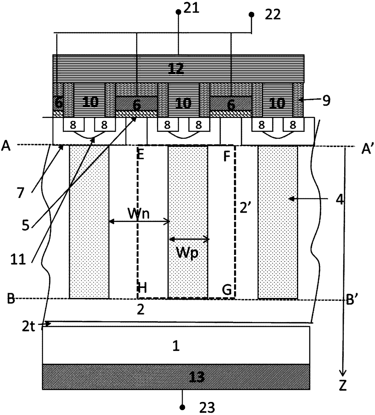
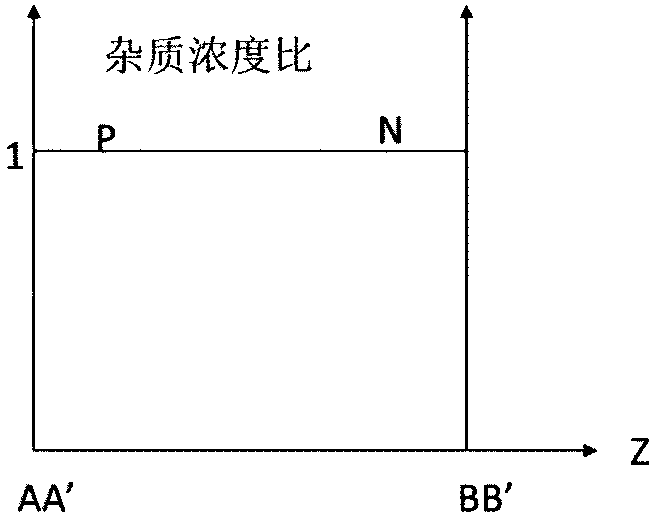
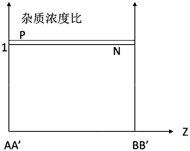
[0065] see Figure 4a , which is a specific embodiment of the super-junction structure of the present invention, which is a super-junction MOSFET (here, NMOSFET) to which the super-junction structure is applied. On the N-type heavily doped silicon substrate 1 is an N-type epitaxial layer 2. Due to the difference in doping concentration, there is a transition region 2t between the heavily doped silicon substrate 1 and the uniform concentration epitaxial layer 2, and the N-type epitaxial layer 2 Layer 2 has a plurality of P-shaped columns 4 . The N-type epitaxial layer 2 between every two adjacent P-type pillars 4 can be regarded as an N-type pillar 2'. In this way, a plurality of P-type pillars 4 and N-type pillars 2' arranged alternately are formed in the N-type epitaxial layer 2, that is, a super-junction structure. The super-junction structure here refers to Figure 4a The area between AA' under the middle p-well 7 and the bottom of the trench BB', such as Figure 4b show...


PUM


Abstract

The invention discloses a super junction structure. A current flow area is composed of P-type columns and N-type columns which are arranged alternately. The P-type columns present non-uniform distribution of impurity, and the N-type columns present uniform or non-uniform distribution of impurity. Finally, in an area close to an N-type heavily doped substrate, the total amount of P-type impurity in the P-type columns is lower than the total amount of N-type impurity in the N-type columns; in an area close to the top of a device, the total amount of P-type impurity in the P-type columns is higher than the total amount of N-type impurity in the N-type columns; and in a quasi charge balance section, the absolute value of the difference between the total amount of impurity in the P-type columns and the total amount of impurity in the N-type columns is smaller than 5% of the total amount of impurity in the N-type columns in the section, and the quasi charge balance section includes a position of complete charge balance. By adopting the super junction structure, the avalanche current tolerance and stability of devices are improved, and the consistency of breakdown voltage of devices is improved. The invention further discloses an MOS field-effect transistor using the structure and a manufacturing method thereof.

Description

technical field [0001] The invention relates to a power semiconductor device, in particular to a super junction semiconductor device. Background technique [0002] A super junction structure is a structure of alternately arranged N-shaped pillars and P-shaped pillars. If the superjunction structure is used to replace the N-type drift region in the VDMOS (Vertical Double-diffused Metal-Oxide-Semiconductor, vertical double-diffused MOS transistor) device, a conduction path is provided in the conduction state (only the N-type column provides a path, The P-type column is not provided), and bears the reverse bias voltage in the off state (the PN column is jointly borne), forming a super junction MOSFET (Metal-Oxide-Semiconductor Field-Effect Transistor, MOSFET, Metal-Oxide Semiconductor Field-Effect Transistor) . The super-junction MOSFET can greatly reduce the on-resistance of the device by using a low-resistivity epitaxial layer when the reverse breakdown voltage is consisten...

Claims


Application Information

Patent Timeline
Patent Type & Authority Patents(China)
IPC IPC(8): H01L29/06H01L21/336H01L29/78
CPCH01L29/0634H01L29/66484H01L29/66666H01L29/7828H01L29/7831
Inventor 肖胜安
Owner SHENZHEN SANRISE TECH CO LTD
Why Eureka
Try Eureka