A kind of microbridge structure of broadband and high absorption of terahertz wave and preparation method thereof

A microbridge structure and terahertz technology, applied in the field of room temperature terahertz detection array imaging, can solve the problem of low responsivity, achieve the effect of improving the responsivity, overcoming low terahertz radiation absorption and narrow spectral response

Inactive Publication Date: 2017-08-11
UNIV OF ELECTRONICS SCI & TECH OF CHINA
View PDF6 Cites 0 Cited by
  • Summary
  • Abstract
  • Description
  • Claims
  • Application Information

AI Technical Summary

Problems solved by technology

[0005] The purpose of the present invention is to solve the problem of low response rate of current terahertz detectors in the wide frequency band, to design a micro-bridge structure with wide band and high absorption of terahertz waves and its preparation method, so as to realize wide spectrum and high detection of terahertz waves. Absorption, improving the response rate of the microbridge structure detection unit to terahertz waves

Method used


Image

  • A kind of microbridge structure of broadband and high absorption of terahertz wave and preparation method thereof
  • A kind of microbridge structure of broadband and high absorption of terahertz wave and preparation method thereof
  • A kind of microbridge structure of broadband and high absorption of terahertz wave and preparation method thereof

Examples


Embodiment Construction

[0023] The present invention will be described in further detail below in conjunction with the accompanying drawings and embodiments.

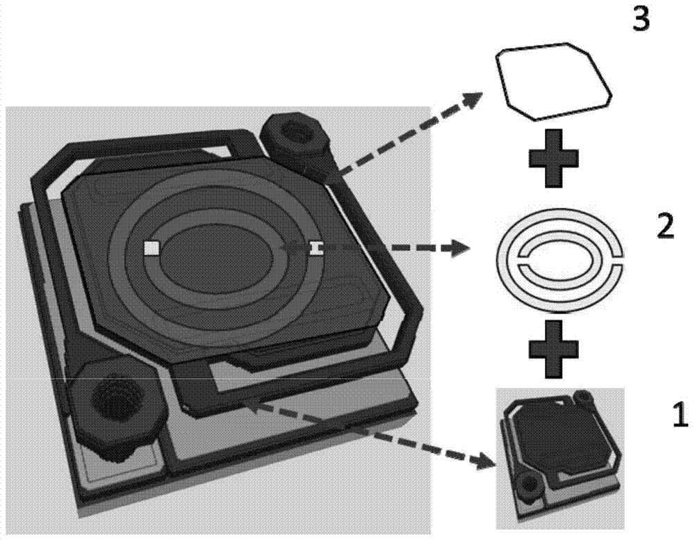
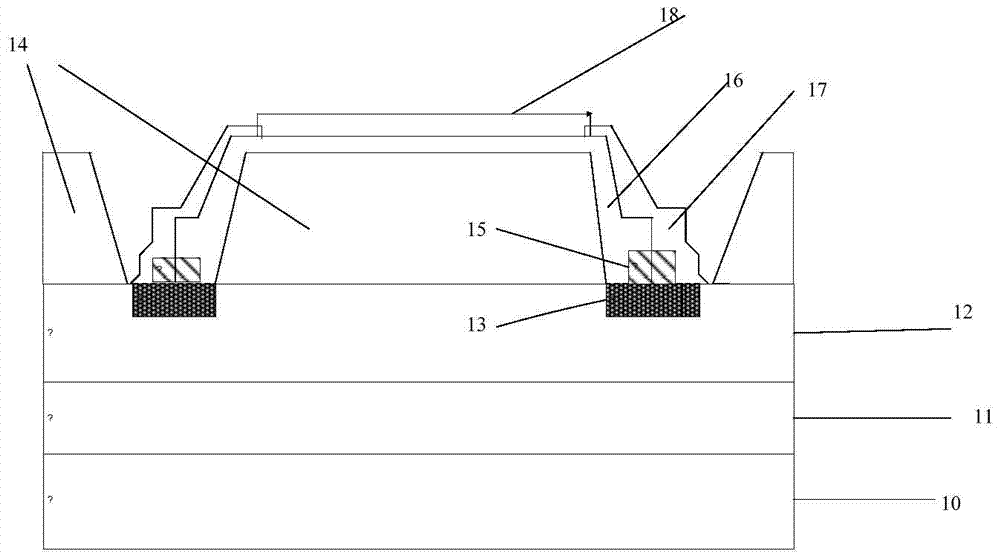
[0024] In this embodiment, the microbridge structure with broadband and high absorption of terahertz waves is as follows figure 1 As shown, it includes a metal absorption film 3 on the top layer, a metamaterial pattern 2 on the middle layer, a MEMS microbridge 1 on the bottom layer, and a silicon nitride dielectric layer spacer is set between the two; the metal absorption film is an impedance matching The nano-scale metal absorption film Ti is used for terahertz wave broadband absorption; the MEMS microbridge is as Figure 2-a As shown, it includes a substrate 10, a driving circuit 11, a metal aluminum reflective layer 12, and a bridge deck supported on the metal aluminum reflective layer by bridge legs. The bridge deck includes a supporting layer 16, a top electrode 17, and a vanadium oxide film ( Sensitive material layer) 18, support layer ...


PUM

PropertyMeasurementUnit
thicknessaaaaaaaaaa
thicknessaaaaaaaaaa

Abstract

The invention belongs to the technical field of room temperature terahertz detection array imaging, and provides a wide-band high-absorption terahertz wave microbridge structure and a preparation method thereof, which are used to overcome the problem of low response rate of a terahertz detector in a wide frequency band. The microbridge structure includes a metal absorption film on the top layer, a metamaterial pattern on the middle layer, and a MEMS microbridge on the bottom layer, and a silicon nitride dielectric layer spacer is set between the two; the metal absorption film is an impedance-matched nano A level metal absorption film, the metamaterial pattern and the MEMS micro bridge together constitute a metamaterial absorption structure. In the present invention, the impedance-matched nanoscale metal absorption film can realize broadband absorption of terahertz waves, and the metamaterial pattern and MEMS microbridge structure together constitute a metamaterial absorption structure that can ensure high absorption of terahertz waves; realize terahertz waves The performance of wide spectral response and high absorption improves the responsivity of the microbridge structure detection unit to terahertz waves as a whole.

Description

technical field [0001] The invention belongs to the technical field of terahertz detection array imaging at room temperature, and in particular relates to a wide-band high-absorption terahertz wave microbridge structure and a preparation method thereof. Background technique [0002] Terahertz waves often refer to electromagnetic waves with a frequency of 0.1THz to 10THZ (wavelength 3mm to 30μm). Due to the special frequency band, which belongs to the transition range between macroelectronics and microphotonics, THz waves exhibit a series of unique properties different from other frequency band electromagnetic waves, making them widely used in military and civilian fields (such as imaging, communication, remote sensing, Radar, astronomy, biomedicine, etc.) have important scientific research value and wide application. Compared with other waves, terahertz waves have the following characteristics: (1) The frequency range of terahertz radiation is very wide, which almost covers...

Claims


Application Information

Patent Timeline
Patent Type & Authority Patents(China)
IPC IPC(8): B81B1/00B81B7/02B81C1/00G01J1/42
Inventor 王军陈沛丞谢盼云唐荣黎威志
Owner UNIV OF ELECTRONICS SCI & TECH OF CHINA
Why Eureka
Try Eureka