Multilayer cascaded photocathode with wide spectral response and preparation method thereof

A photocathode, wide-spectrum technology, applied in the manufacturing of light-emitting cathodes, photo-emission cathodes, main electrodes of discharge tubes, etc., can solve the problems of no photoelectric response, short wavelength limit of materials, etc., to achieve favorable migration and emission, wide-spectrum response , the effect of increasing the diffusion length

Active Publication Date: 2021-05-07
NANJING UNIV OF SCI & TECH
View PDF7 Cites 0 Cited by
  • Summary
  • Abstract
  • Description
  • Claims
  • Application Information

AI Technical Summary

Problems solved by technology

The disadvantage of GaAs material is that the material has almost no photoelectric response to ultraviolet and infrared bands.
However, the long-wavelength limit of this material is too short, and the spectral response range is mainly concentrated in the ultraviolet band.

Method used


Image

  • Multilayer cascaded photocathode with wide spectral response and preparation method thereof
  • Multilayer cascaded photocathode with wide spectral response and preparation method thereof
  • Multilayer cascaded photocathode with wide spectral response and preparation method thereof

Examples


preparation example Construction

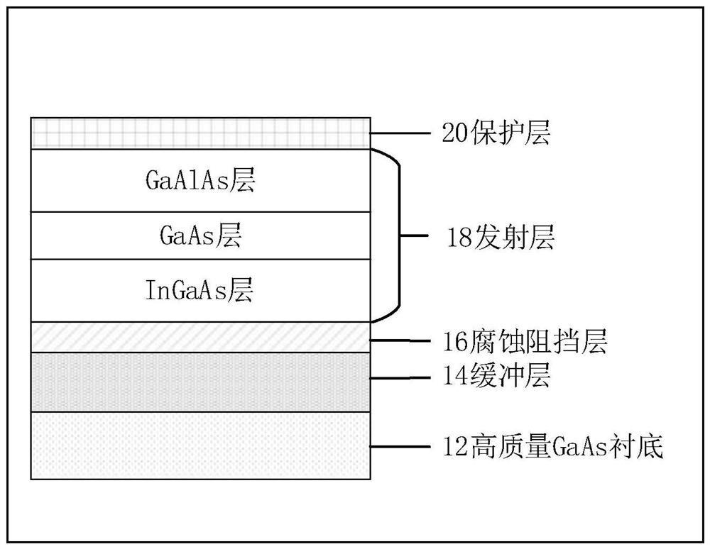
[0032] The present invention also provides a method for preparing a multi-layer cascaded wide-spectrum response photocathode, the specific steps are:

[0033] Step 1. On the substrate, sequentially grow the InGaAs buffer layer, p-type Al 0.8 In 0.2 As corrosion barrier layer, p-type emitter layer In x Ga 1-x As part, p-type emission layer GaAs part, p-type emission layer Ga 1-y al y As part and protective layer;

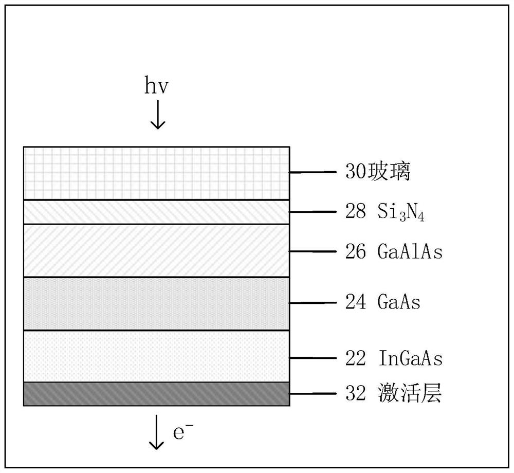
[0034] Step 2, corrode the protection layer with a chemical etchant, the Ga in the emitter layer 0.1 al 0.9 A layer of Si is deposited on the upper surface of the As layer 3 N 4 antireflective coating, then the Si 3 N 4 Thermally bonded countertop glazing on anti-reflective film;

[0035] Step 3, sequentially corrode the substrate, In x Ga 1-x As buffer layer, p-type Al 0.8 In 0.2 As corrosion barrier layer, exposed In in the emitter layer x Ga 1-x As surface;

[0036] Step 4, through the ultra-high vacuum activation process, on the surface of the e...

Embodiment

[0039] A multilayer cascaded photocathode with wide spectral response, including a bottom-up substrate, an InGaAs buffer layer, a p-type Al 0.8 In 0.2 As corrosion barrier layer, p-type emission layer and protective layer, wherein, the p-type emission layer comprises p-type In x Ga 1-x As layer, p-type GaAs layer, p-type Ga 1-y al y As layer.

[0040] In x Ga 1-x The In composition of the As buffer layer increases from bottom to top layer by layer from 0 to 0.2, wherein the thickness of each layer is 1 μm, and the total thickness of the buffer layer is 4 μm.

[0041] p-type Al 0.8 In 0.2 The In composition in As is 0.2, and the doping concentration is 3×10 17 cm -3 . The total thickness of the corrosion barrier layer is 1 μm.

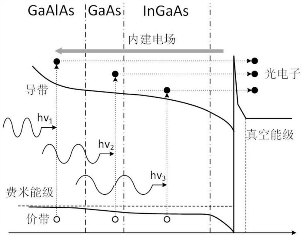
[0042] Such as image 3 As shown, the emission layer is divided into three sub-layers, namely In x Ga 1-x As layer, GaAs layer, Ga 1-y al y As layer. where In x Ga 1-x The As layer is divided into four layers with different In compo...


PUM

PropertyMeasurementUnit
thicknessaaaaaaaaaa
thicknessaaaaaaaaaa
thicknessaaaaaaaaaa

Abstract

The present invention proposes a multilayer cascaded wide-spectrum response photocathode and its preparation method. The photocathode includes a substrate arranged from bottom to top, an InGaAs buffer layer, a p-type Al 0.8 In 0.2 As corrosion barrier layer, p-type emission layer and protective layer, wherein, the p-type emission layer comprises p-type In x Ga 1‑x As layer, p-type GaAs layer, p-type Ga 1‑y al y As layer. In the emitter layer, In x Ga 1‑x In the As part, the In composition x decreases from 0.2 to 0.05 layer by layer from bottom to top, and the doping method of the GaAs layer is a variable doping distribution. 1‑ y al y The Al composition y in the As part increases from 0 to 0.9 layer by layer from bottom to top. The present invention adopts variable composition and variable doping technology in the emission layer, on the one hand, it increases the diffusion length of the photogenerated electrons in the emission layer, helps the photogenerated electrons to migrate to the emission surface, and is more conducive to the emission of the photogenerated electrons.

Description

technical field [0001] The invention belongs to the technical field of low-light night vision detection materials, in particular to a multi-layer cascaded wide-spectrum response photocathode and a preparation method thereof. Background technique [0002] Since Koller and Campbell invented the Ag-O-Cs(S1) photocathode in 1929, in the long-term research, more and more photocathode materials have been discovered, but each material always has Certain differences and characteristics. At the end of the twentieth century, InGaAs photocathode got more attention. Before that, there were few researches on near-infrared sensitive III-V semiconductor materials. In past studies, people have proposed a photocathode with GaAlAs as the window layer and InGaAs as the emission layer, and a photocathode with InAlAs as the window layer and InGaAs as the emission layer. However, it was found in the experiment that the GaAlAs window layer did not match the lattice coefficient of InGaAs well, an...

Claims


Application Information

Patent Timeline
Patent Type & Authority Patents(China)
IPC IPC(8): H01J1/34H01J9/12
Inventor 张益军王自衡张景智钱芸生荣敏敏方城伟戴庆鑫康天佑张锴珉舒昭鑫
Owner NANJING UNIV OF SCI & TECH
Why Eureka
Try Eureka