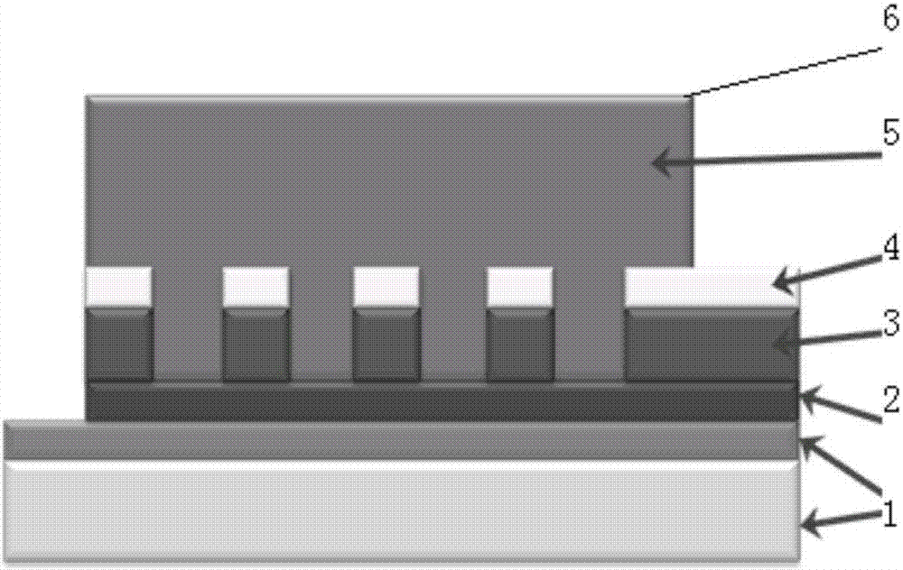
A back contact perovskite solar cell
A solar cell and perovskite technology, applied in the field of solar cells, can solve the problems of poor stability, restricted practicality, low conversion efficiency of perovskite cells, etc., and achieve the effect of improving conversion efficiency and reducing shading loss
- Summary
- Abstract
- Description
- Claims
- Application Information
AI Technical Summary
Problems solved by technology
Method used
Image
Examples
Embodiment 1
[0024] 1) Substrate 1 is made of FTO transparent conductive glass, and its sheet resistance is ~15Ω / □
[0025] 2) Electron transport layer 2 is made of magnetron sputtered ZnO with a thickness of ~100nm, heat-treated at 400°C and N2 atmosphere for 1h
[0026] 3) The original diameter of the PS beads used is 2um, and the monodisperse layer PS beads are laid by the liquid surface monodisperse layer transfer method, and the monodisperse layer PS beads have a hexagonal close-packed structure.
[0027] 4) Use RIE dry etching to reduce the diameter of PS pellets to 1um
[0028] 5) Al2O3 is prepared by ALD method for the dielectric layer 3, with a thickness of ~50nm
[0029] 6) The metal layer 4 is made of magnetron sputtering Au, with a thickness of ~40nm
[0030] 7) Use toluene ultrasonic to peel off the Al2O3 and Au on the PS ball and its top to form a mesh structure of Al2O3 and Au. The mesh period length is 2um, the mesh diameter is ~1um, and the mesh is also arranged in a hex...
PUM
 Abstract
Description
Claims
Application Information
