Substrate, making method of substrate and display device adopting substrate

A manufacturing method and a technology of a substrate, which are applied to instruments, electrical digital data processing, and the input/output process of data processing, etc., can solve problems such as increasing the width of substrate grounding traces, easy peeling of grounding traces, etc., and improve display quality , increase adhesion, reduce the effect of transmission resistance

Inactive Publication Date: 2015-12-23
BOE TECH GRP CO LTD +1
View PDF5 Cites 21 Cited by
  • Summary
  • Abstract
  • Description
  • Claims
  • Application Information

AI Technical Summary

Problems solved by technology

[0004] The invention provides a substrate, a manufacturing method thereof, and a display device, which are used to solve the problem that the gro

Method used


Image

  • Substrate, making method of substrate and display device adopting substrate
  • Substrate, making method of substrate and display device adopting substrate
  • Substrate, making method of substrate and display device adopting substrate

Examples


Example Embodiment

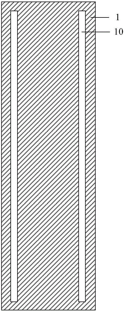
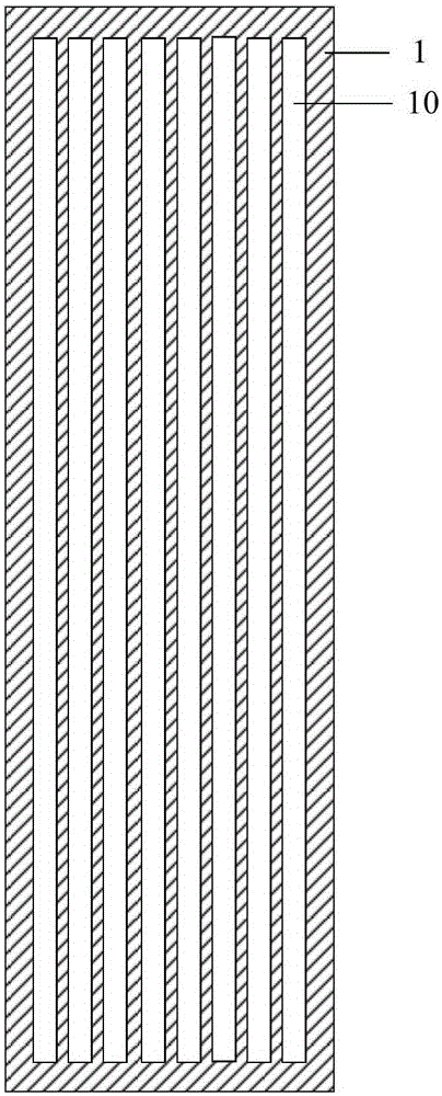
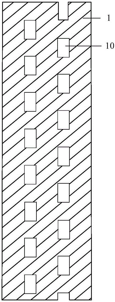
[0020] During the production process of substrates, such as array substrates and color film substrates, static electricity will be introduced. When static electricity with a very high voltage enters the signal line, it will cause electrostatic breakdown of the signal line and form an open circuit, resulting in the inability to transmit the signal and seriously affecting performance of the substrate. In order to avoid the above situation, ground traces are designed on the edge of the substrate. Connect the ground trace to the signal line, or use the tip discharge principle to discharge the static electricity accumulated on the signal line. Low transfer resistance is conducive to the rapid discharge of static electricity from the ground trace. In the prior art, the resistance value of the grounding wire is reduced by increasing the line width of the grounding wire, but this will reduce the adhesion of the grounding wire, and the phenomenon of peeling of the grounding wire is pr...


PUM


Abstract

The present invention relates to the technical field of display, and discloses a substrate, a making method of the substrate and a display device adopting the substrate. The substrate comprises a signal line and a grounding route. The grounding route is used for discharging static electricity on the signal line; by making a plurality of hollowed areas on the grounding route, line widths of the grounding route in the corresponding areas can be reduced, an adhesion force of the grounding route is increased and the grounding route is prevented from being peeled off. Meanwhile, the grounding route also can be guaranteed to have a certain line width, transmission resistance is reduced, and the static electricity accumulated on the signal line is rapidly discharged, thereby ensuring substrate performance and improving display quality of the display device.

Description

technical field [0001] The invention relates to the field of display technology, in particular to a substrate, a manufacturing method thereof, and a display device. Background technique [0002] On the display substrate, the line width of the signal line used to transmit signals is usually small, generally 30um, 25um, 20um. When static electricity with a very high voltage enters the signal line, it will cause electrostatic breakdown of the signal line, forming Open circuit, causing the signal cannot be transmitted. Therefore, in order to avoid such a situation, a ground (GND) wiring is generally designed at the edge of the display substrate, in order to quickly discharge static electricity. [0003] Usually the line width of the GND line is 300um ~ 400um. Of course, the larger the line width of the GND line, the better. In this case, the resistance will be very low, and the static electricity can be quickly released. However, when the line width of the GND trace is designe...

Claims


Application Information

Patent Timeline
IPC IPC(8): G06F3/041
CPCG06F3/041G06F2203/04103G06F2203/04107
Inventor 谢晓冬胡明张明陈军涛田健
Owner BOE TECH GRP CO LTD
Why Eureka
Try Eureka