Cleaning agent for metal wiring substrate, and method for cleaning semiconductor substrate
A metal wiring and cleaning agent technology, applied in chemical instruments and methods, semiconductor/solid-state device manufacturing, preparation of detergent mixture compositions, etc., can solve the problems of longer standby time of substrates and increased standby status of substrates, etc. Achieve effective and stable cleaning, not easy to deteriorate
- Summary
- Abstract
- Description
- Claims
- Application Information
AI Technical Summary
Problems solved by technology
Method used
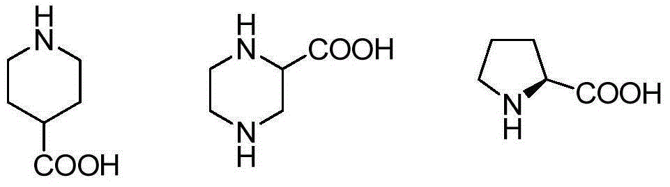
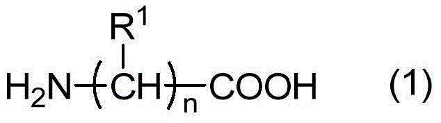
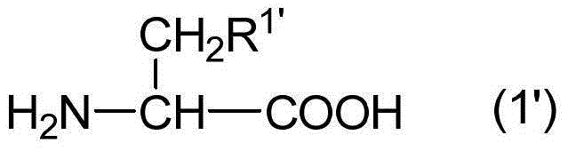
Image

Examples
Embodiment
[0079] Hereinafter, although this invention is demonstrated concretely based on an Example and a comparative example, this invention is not limited to these examples. In addition, unless otherwise specified, the % which exists in the following example means a weight basis (w / w%).
[0080] -Evaluation of the manufacturing method of substrate A-
[0081] Purchased wafers were planarized by polishing the surface of Sematech 845 (copper wiring, barrier metal TaN, oxide film TEOS; manufactured by Sematech) with a diameter of 8 inches with a polishing slurry containing benzotriazole (BTA) Wafers rinsed with pure water. The wafer was dipped in a 1% benzotriazole (BTA) aqueous solution for 1 hour to form a copper (I)-benzotriazole film on the surface of the copper wiring, and then cleaned with a single-wafer cleaner (KAIJO Multi- Spinner) for pure water washing and spin drying. Next, this wafer was chipped to about 2 cm×2 cm, and used as an evaluation substrate A.
[0082] -Evalua...
PUM
| Property | Measurement | Unit |
|---|---|---|
| diameter | aaaaa | aaaaa |
| diameter | aaaaa | aaaaa |
| particle diameter | aaaaa | aaaaa |
Abstract
Description
Claims
Application Information
 - R&D
- Intellectual Property
- Life Sciences
- Materials
- Tech Scout
- Unparalleled Data Quality
- Higher Quality Content
- 60% Fewer Hallucinations
Browse by: Latest US Patents, China's latest patents, Technical Efficacy Thesaurus, Application Domain, Technology Topic, Popular Technical Reports.
© 2025 PatSnap. All rights reserved.Legal|Privacy policy|Modern Slavery Act Transparency Statement|Sitemap|About US| Contact US: help@patsnap.com