Photovoltaic Module Crystalline Silicon Cell Welding Process
A technology of crystalline silicon cells and photovoltaic modules, which is applied in photovoltaic power generation, welding equipment, circuits, etc., can solve the problems of increased welding difficulty, prone to false welding, and low welding efficiency, and achieves improved welding reliability and poor solder joints. Rate reduction, the effect of achieving lead-free soldering
- Summary
- Abstract
- Description
- Claims
- Application Information
AI Technical Summary
Problems solved by technology
Method used
Image
Examples
Embodiment 1
[0038] Embodiment 1: a photovoltaic module cell sheet welding process, comprising the following steps:
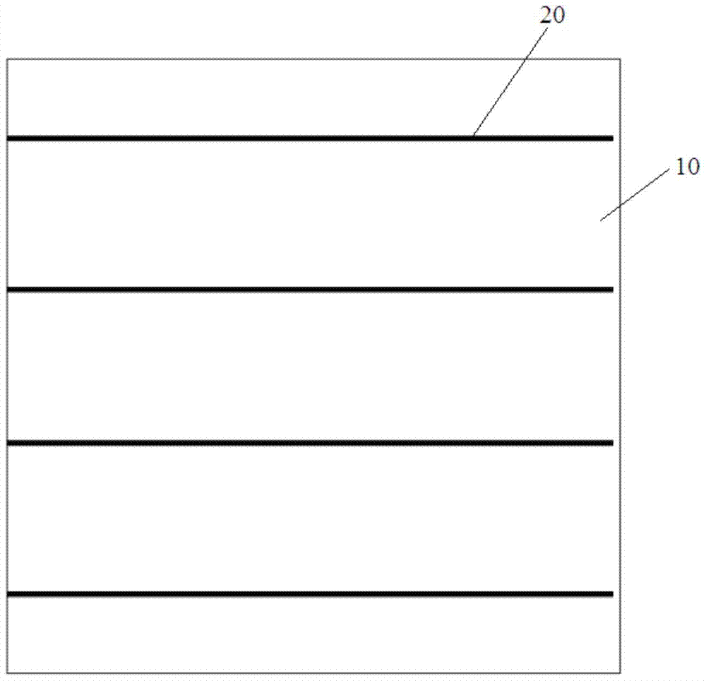
[0039] (1) Solder paste printing: such as figure 1 As shown, solder paste 20 (which may be leaded solder paste or more environmentally friendly lead-free solder paste) is printed on the busbar on the surface of the battery sheet 10 using a solder paste printer; the battery sheet 10 may be a conventional battery sheet, HIT cell or bifacial cell; MWT / IBC back contact cell can also be used, such as Figure 17 As shown, the graphic of the screen printing template is designed according to the main grid graphic and size of the cell;
[0040] (2) Ribbon placement: Use a placement machine to accurately place the conductive ribbon 30 (which may be lead-containing ribbon or a more environmentally friendly lead-free ribbon) on the main grid line of the battery sheet 10 On the solder paste 20, a plurality of battery sheets 10 are connected in series through a solder ribbon 30, specif...
Embodiment 2
[0047] Embodiment 2: a photovoltaic module cell sheet welding process, comprising the following steps:
[0048] (1) Solder paste printing: such as figure 1 As shown, the busbars on the surface of the battery sheet 10 are printed with solder paste 20 (which may be leaded solder paste or more environmentally friendly lead-free solder paste) using a solder paste printing machine;
[0049] (2) Ribbon placement: Use a placement machine to accurately place the conductive ribbon 30 (which may be lead-containing ribbon or a more environmentally friendly lead-free ribbon) on the main grid line of the battery sheet 10 On the solder paste 20, a plurality of battery sheets 10 are connected in series through a solder ribbon 30, specifically as image 3 As shown; the solder strip 30 can be tinned solder strip or pure copper strip, and the surface of the pure copper strip does not need to be tinned; as figure 2 As shown, the welding surface S1 and the non-welding surface S2 are circularly...
Embodiment 3
[0055] Embodiment three: a photovoltaic module cell sheet welding process, comprising the following steps:
[0056] (1) Solder paste printing: such as figure 1 As shown, the busbars on the surface of the battery sheet 10 are printed with solder paste 20 (which may be leaded solder paste or more environmentally friendly lead-free solder paste) using a solder paste printing machine;
[0057] (2) Ribbon placement: Use a placement machine to accurately place the conductive ribbon 30 (which may be lead-containing ribbon or a more environmentally friendly lead-free ribbon) on the main grid line of the battery sheet 10 On the solder paste 20, a plurality of battery sheets 10 are connected in series through a solder ribbon 30, specifically as image 3 As shown; the solder strip 30 can be tinned solder strip or pure copper strip, and the surface of the pure copper strip does not need to be tinned; as figure 2 As shown, the welding surface S1 and the non-welding surface S2 are circul...
PUM
| Property | Measurement | Unit |
|---|---|---|
| depth | aaaaa | aaaaa |
| height | aaaaa | aaaaa |
| length | aaaaa | aaaaa |
Abstract
Description
Claims
Application Information


