Pixel compensation circuit and drive method thereof, array substrate and display device

A compensation circuit and pixel technology, applied in static indicators, instruments, etc., can solve problems such as different currents, affecting display effects, uneven threshold voltage of driving thin film transistors, etc., achieve the effect of fewer signal lines and avoid the influence of driving current

Inactive Publication Date: 2016-01-13
BOE TECH GRP CO LTD +1
View PDF5 Cites 24 Cited by
  • Summary
  • Abstract
  • Description
  • Claims
  • Application Information

AI Technical Summary

Problems solved by technology

[0008] 5. Both AMOLED and SUPERAMOLED have a very wide color gamut, but color cast
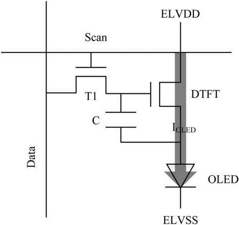
In the existing driving circuit, there is non-uniformity in the threshold voltage of the driving thin-film transistor of each pixel driving the light-emi

Method used


Image

  • Pixel compensation circuit and drive method thereof, array substrate and display device
  • Pixel compensation circuit and drive method thereof, array substrate and display device
  • Pixel compensation circuit and drive method thereof, array substrate and display device

Examples


Embodiment Construction

[0030] The present invention will be fully described below with reference to the accompanying drawings showing embodiments of the invention. However, this invention may be embodied in many different forms and should not be construed as limited to the embodiments set forth herein. Rather, these embodiments are provided so that this disclosure will be thorough and complete, and will fully convey the scope of the invention to those skilled in the art. In the drawings, components are exaggerated for clarity.

[0031] It should be understood that although the terms first, second, third etc. may be used herein to describe various elements, components and / or sections, these elements, components and / or sections should not be limited by these terms. These terms are only used to distinguish one element, component or section from another. Thus, a first element, component or section discussed below could be termed a second element, component or section without departing from the teachin...


PUM


Abstract

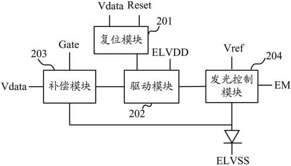
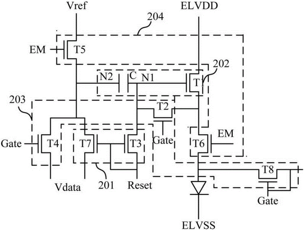
Disclosed are a pixel compensation circuit and a drive method thereof, an array substrate and a display device. The pixel compensation circuit comprises a reset module (201), a drive module (202), a compensation module (203) and a light-emitting control module (204); the reset module (201) is connected with a reset signal line and the drive module, and is configured to reset the drive module according to a reset signal input by the reset signal line; the drive module (202) is configured to output a drive current to drive light-emitting display of a display device; the compensation module (203) is connected with a signal control line, a data line and the drive module, and is configured to perform threshold voltage compensation and data write-in for the drive module under the control of a signal control signal input by the signal control line; and the light-emitting control module (204) is connected with a light-emitting control line, the drive module and the anode of the display device, and is configured to control the drive module to drive the light-emitting display of the display device according to a light-emitting control signal input by the light-emitting control line. The pixel compensation circuit can effectively prevent an influence of a threshold voltage on a drive current, and the pixel compensation circuit has less signal lines so that the fact that the pixel compensation circuit is used in mask design of a TFT substrate in a high-resolution display screen is facilitated.

Description

technical field [0001] The present disclosure relates to the field of active-matrix organic light-emitting diode displays, and more specifically, to a pixel compensation circuit for active-matrix organic light-emitting diode panel displays and a driving method thereof, an array substrate including the pixel compensation circuit, and a corresponding display device. Background technique [0002] AMOLED (Active-matrixorganiclight-emittingdiode, active-matrix organic light-emitting diode or active-matrix organic light-emitting diode) is a display technology used in TVs and mobile devices. The use of AMOLED technology as a display screen has been loved by customers and has been well received. At the same time, it has also opened up the next display technology AMOLED involving LTPS-LCD (Low Temperature Poly-silicon Liquid Crystal Display). [0003] Compared with traditional display technology, AMOLED has the following advantages: [0004] 1. Compared with the liquid crystal cell...

Claims


Application Information

Patent Timeline
IPC IPC(8): G09G3/32
CPCG09G3/3233G09G2300/0819G09G2300/0842G09G2300/0861G09G2320/045G09G3/3258G09G3/3266G09G3/3291G09G2300/043G09G2300/0809G09G2310/061G09G2320/0646
Inventor 王博玄明花马占洁
Owner BOE TECH GRP CO LTD
Why Eureka
Try Eureka