Physical unclonable chip circuit

A circuit and chip technology, applied in the field of information security, can solve the problems of high power consumption, large area overhead, and restrictions on the application of PUF chips, and achieve the effect of low power consumption and reduced area

Inactive Publication Date: 2016-01-13
SHENZHEN UNIV
View PDF2 Cites 23 Cited by
  • Summary
  • Abstract
  • Description
  • Claims
  • Application Information

AI Technical Summary

Problems solved by technology

So this approach can reduce power consumption to a certain extent, but its implementation still requires a lot of area overhead
[0010] The digital-analog hybrid PUF chips disclosed in literature [1-3] generally have the disadvantages of relatively large area and relatively high power consumption (power

Method used


Image

  • Physical unclonable chip circuit
  • Physical unclonable chip circuit
  • Physical unclonable chip circuit

Examples


Embodiment Construction

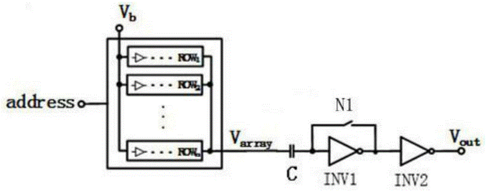
[0024] The structure and principle of the physically unclonable chip circuit in the embodiment of the present invention are as follows: Figure 1 to Figure 3 shown.

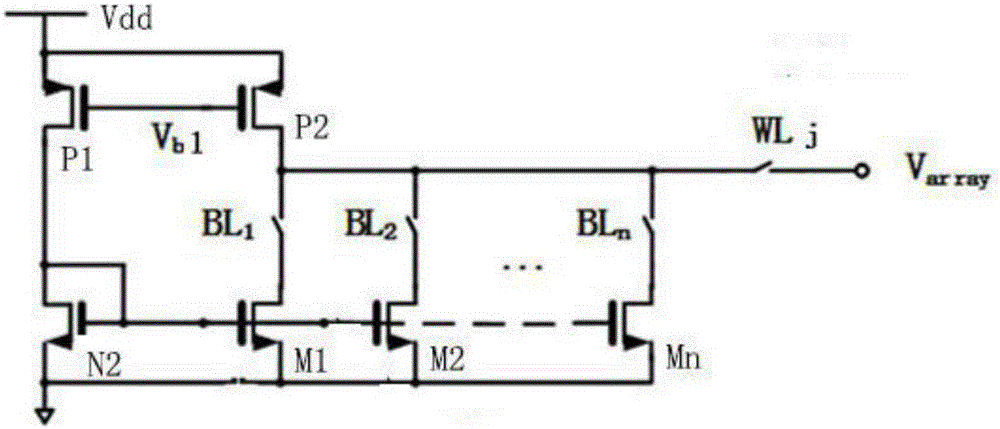
[0025] The physical non-clonable chip circuit and architecture of the embodiment of the present invention are as follows: figure 1 As shown, the physical non-clonable chip circuit consists of M rows and N columns of MOSFET arrays operating in the sub-threshold region and an automatic zero-calibration comparator. The array is composed of M×N minimum size NMOS with PMOS as the load.

[0026] The input signal of the physically unclonable chip circuit will select a row address port WL after being decoded by the decoder. j and a column address port BL i . by selected BL i and selected WL j One of the corresponding NMOSs can be turned on, and this NMOS will form a unipolar CMOS amplifier with the load PMOS in the row. The MOSFET array is connected from V array The terminals output voltages with different voltage...


PUM


Abstract

The invention discloses a physical unclonable chip circuit. The physical unclonable chip circuit comprises M rows and N columns of MOSFET (Metal-Oxide-Semiconductor-Field-Effect Transistor) arrays and automatic zeroing comparators, which work in a sub-threshold region, wherein each MOSFET array comprises M rows and N columns of NMOSs (N-Metal-Oxide-Semiconductor) with PMOSs (P-channel Metal Oxide Semiconductor) as loads; after an input signal of the physical unclonable chip circuit is decoded, the corresponding NMOSs are selected for conduction, the selected NMOSs and the load PMOSs in the corresponding row form a monopole CMOS (Complementary Metal-Oxide-Semiconductor) amplifier, and output ends of the MOSFET arrays output voltages with different voltage values in sequence; each automatic zeroing comparator continuously compares a previous voltage and a latter voltage which are output by each MOSFET array, and during a process for subsequent comparison, an output end of each automatic zeroing comparator outputs a response signal of the physical unclonable chip circuit. The physical unclonable chip circuit adopts the single-stage amplifier as a unit circuit of each array, and has the advantages of small chip area, low power consumption and wide application range.

Description

[technical field] [0001] The invention relates to the field of information security, in particular to a physically unclonable chip circuit. [Background technique] [0002] Physical Unclonable Function (Physical UnclonableFunction, PUF) is a function constructed according to the inherent small differences introduced by physical entities when they are realized. This function changes due to the intrinsic physical differences of the entities, and it can realize the function of applying the same input to different entities but giving different outputs. Therefore, this function can be used to implement circuit chip signature technology. In addition, the PUF circuit can also be used for key generation of public key encryption systems, smart card key identification systems, radio frequency identification systems (Radio Frequency Identification, RFID) and related intellectual property protection. At the same time, according to the way integrated circuits are implemented, it can be ...

Claims


Application Information

Patent Timeline
IPC IPC(8): H03K19/094
Inventor 赵晓锦林仕傍彭亮多
Owner SHENZHEN UNIV
Why Eureka
Try Eureka