Integrated transformer

A technology that integrates transformers and metal layers. It is applied in the direction of electric solid-state devices, semiconductor devices, semiconductor/solid-state device components, etc., and can solve the problems of large chip area and consumption.

Active Publication Date: 2016-01-27
REALTEK SEMICON CORP
View PDF4 Cites 3 Cited by
  • Summary
  • Abstract
  • Description
  • Claims
  • Application Information

AI Technical Summary

Problems solved by technology

However, passive components in integrated circuits, such as inductors and transformers, often consume a large amount of chip area. Therefore, how to simplify the number of passive components in integrated circuits, min

Method used


Image

  • Integrated transformer
  • Integrated transformer
  • Integrated transformer

Examples


Embodiment Construction

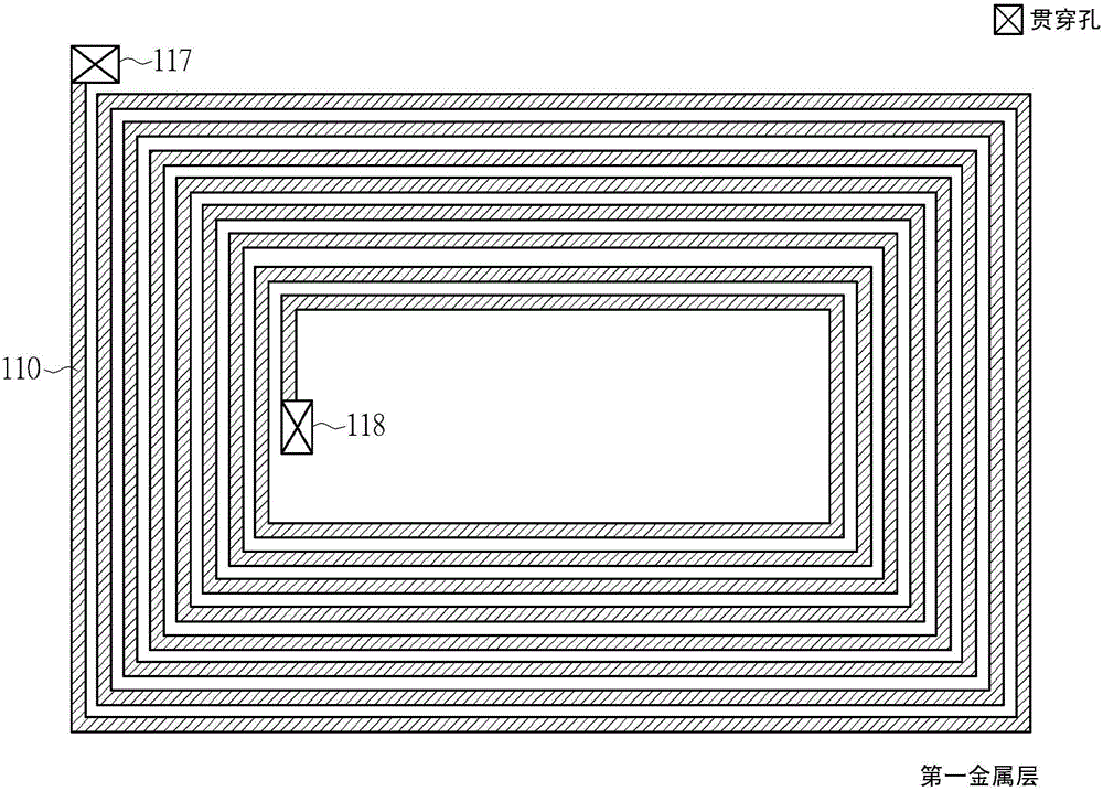
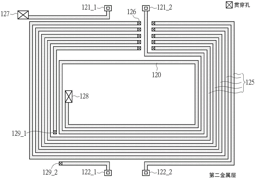
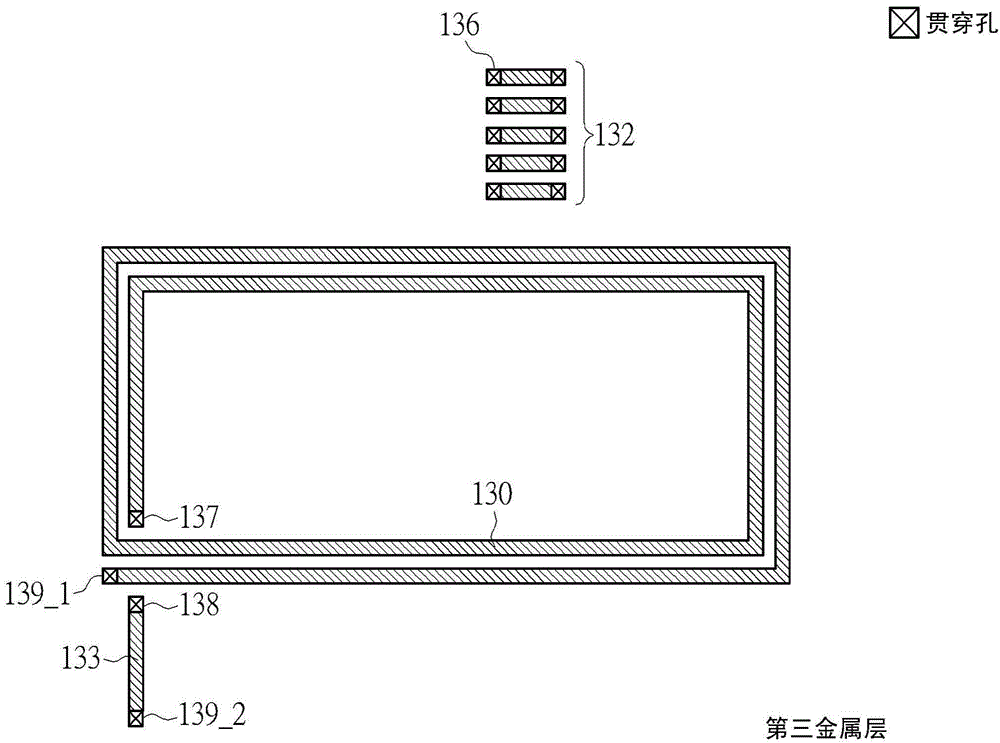
[0028] Please refer to Figure 1A , Figure 1B , Figure 1C , Figure 1D and Figure 1E ,in Figure 1A , 1B and 1C are schematic diagrams of the first metal layer, the second metal layer and the third metal layer of the integrated transformer according to the first embodiment of the present invention, Figure 1D is a top view of the integrated transformer according to the first embodiment of the present invention, Figure 1E It is a sectional view of this embodiment. The integrated transformer of this embodiment can be applied to a transformer or a balanced / unbalanced transformer (balun) in a radio frequency chip.

[0029] In this embodiment, the integrated transformer is an asymmetric integrated transformer (asymmetric integrated transformer), and the ratio of the inductance values ​​of the two inductors is about 9nH: 6nH (nano-Henry) (just an example, not a limitation of the present invention), and The entire integrated transformer has a very small chip area, about 150...


PUM


Abstract

An integrated transformer comprises a first inductor and a second inductor, the first inductor comprises B circles of spiral wirings formed by a first metal layer and A circles of wirings formed by a second metal layer, and the A circles of the wirings formed by the second metal layer is overlapped with the innermost A circles of the wirings of the B circles of the spiral wirings formed by the first metal layer; and the second inductor comprises C circles of wirings formed by at least the second metal layer, the C circles of the wirings, formed by the second metal layer, of the second inductor are substantially overlapped with the partial wirings formed by the first metal layer, A is less than B, and A is less than C.

Description

technical field [0001] The invention relates to an integrated transformer, in particular to an asymmetric integrated transformer. Background technique [0002] Transformers and balanced / unbalanced transformers (balun) are important components used in radio frequency integrated circuits to achieve single-ended to differential signal conversion, signal coupling, impedance matching and other functions. SystemonChip, SoC) development, integrated transformer (integrated transformer / balun) has gradually replaced traditional discrete components, and is widely used in radio frequency integrated circuits. However, passive components in integrated circuits, such as inductors and transformers, often consume a large amount of chip area. Therefore, how to simplify the number of passive components in integrated circuits, minimize the area of ​​passive components, and optimize component characteristics at the same time, such as Quality factor (qualityfactor, Q) and coupling coefficient (c...

Claims


Application Information

Patent Timeline
IPC IPC(8): H01L23/522
Inventor 颜孝璁简育生叶达勋
Owner REALTEK SEMICON CORP
Why Eureka
Try Eureka