
Array substrate and making method thereof

An array substrate and array technology, which is applied in the field of liquid crystal display panel production, can solve problems such as energy waste, and achieve the effects of reducing panel power consumption and improving the utilization rate of backlight sources.

Inactive Publication Date: 2016-02-03
TCL CHINA STAR OPTOELECTRONICS TECH CO LTD
View PDF4 Cites 5 Cited by
  • Summary
  • Abstract
  • Description
  • Claims
  • Application Information

AI Technical Summary

Problems solved by technology

[0003] However, in actual situations, due to the influence of the aperture ratio of pixels in the TFT array and the transmittance of materials (such as polarizers and liquid crystals, etc.), the part of the light emitted by the backlight that finally passes through the panel is only 10% of what is actually generated. left and right, resulting in a great waste of energy

Method used


Image

  • Array substrate and making method thereof
  • Array substrate and making method thereof
  • Array substrate and making method thereof

Examples


Embodiment Construction

[0040] The implementation of the present invention will be described in detail below in conjunction with the accompanying drawings and examples, so as to fully understand and implement the process of how to apply technical means to solve technical problems and achieve technical effects in the present invention. It should be noted that, as long as there is no conflict, each embodiment and each feature in each embodiment of the present invention can be combined with each other, and the formed technical solutions are all within the protection scope of the present invention.

[0041] In order to improve the utilization rate of the light from the backlight source on the liquid crystal display, the photovoltaic effect can be used to convert the light energy of the backlight source which has not been utilized into electrical energy and store it. In the prior art, solar cells are usually arranged at certain positions of the array substrate to convert the light energy of the backlight i...


PUM


Abstract

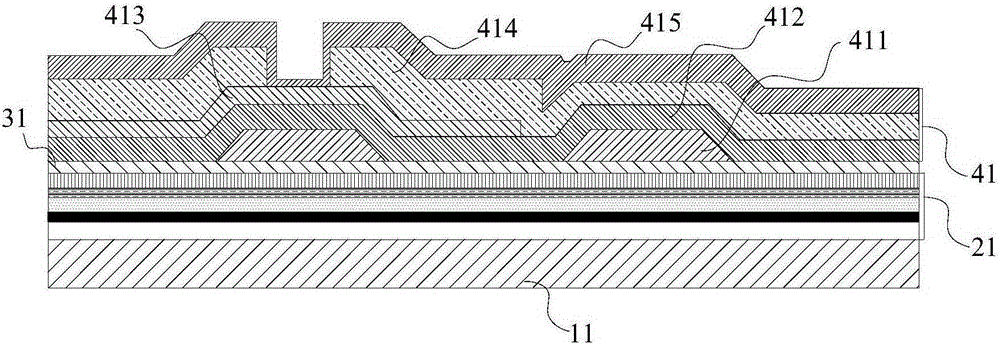
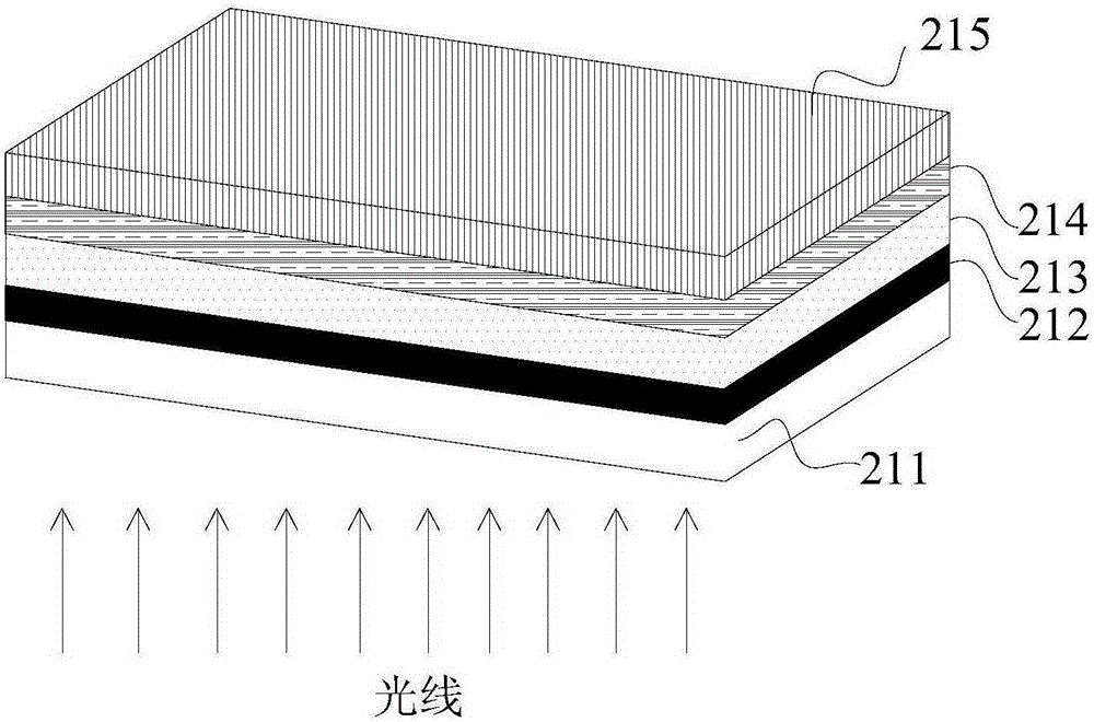
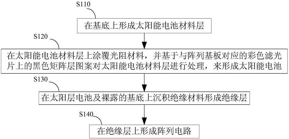
The invention discloses an array substrate and a making method thereof. The array substrate comprises a substrate, a solar cell arranged on the substrate, an insulating layer arranged on the solar cell, and an array circuit arranged on the insulating layer, wherein the solar cell corresponds to a black matrix layer on a color filter corresponding to the array substrate and has the same pattern as the black matrix layer. According to the invention, by arranging the solar cell on the array substrate, backlight energy can be recycled, the utilization rate of backlight can be improved, and the power consumption of the panel can be reduced.

Description

technical field [0001] The present invention relates to the technical field of manufacturing liquid crystal display panels, in particular to an array substrate and a manufacturing method thereof. Background technique [0002] In the working process of TFT-LCD, the incident intensity of the light emitted by the backlight is adjusted to form a gray scale by two layers of polarizers and the liquid crystal sandwiched in it, and the color of the light is adjusted by a color filter to form a color , so as to complete the realistic picture display. [0003] However, in actual situations, due to the influence of the aperture ratio of pixels in the TFT array and the transmittance of materials (such as polarizers and liquid crystals, etc.), the part of the light emitted by the backlight that finally passes through the panel is only 10% of what is actually generated. left and right, resulting in a great waste of energy. Therefore, improving the light utilization rate of the backlight...

Claims


Application Information

Patent Timeline
IPC IPC(8): H01L27/142G02F1/1333
CPCY02E10/50
Inventor 武岳
Owner TCL CHINA STAR OPTOELECTRONICS TECH CO LTD
Learn More