Built-in automatic aging testing device of integrated circuit chips

A technology for integrated circuit and burn-in testing, which is applied in the field of integrated circuit testing and reliability assessment testing. It can solve the problems of high cost and time cost, and achieve the effects of saving time and cost, adjusting the aging voltage, and saving costs.

Inactive Publication Date: 2016-02-10
BEIJING TONGFANG MICROELECTRONICS
View PDF8 Cites 7 Cited by
  • Summary
  • Abstract
  • Description
  • Claims
  • Application Information

AI Technical Summary

Problems solved by technology

The traditional test method above requires an expensive automatic tester and an aging box or an aging box with a test function. The disadvantage is that the cost is high, and if the tester verifies the aging results in real time, it will cause a large amount of time and cost.

Method used


Image

  • Built-in automatic aging testing device of integrated circuit chips
  • Built-in automatic aging testing device of integrated circuit chips

Examples


Embodiment Construction

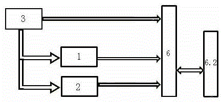
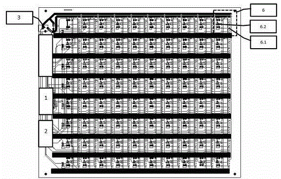
[0015] see figure 1 and figure 2 , The built-in integrated circuit chip automatic aging test device of the present invention includes a reset module 1, a clock signal module 2, a power module 3 and a large number of test units 6 neatly arranged. Each test unit 6 respectively includes a chip holder 6.1 for placing the chip to be tested and a status display light 6.2, and each chip to be tested is equipped with a memory module. The reset module 1 , the clock signal module 2 and the power module 3 are respectively connected to each test unit 6 , and the power module 3 supplies power to the reset module 1 , the clock signal module 2 and each test unit 6 respectively.

[0016] The steps of the test method using the automatic aging test device of the above-mentioned embodiments of the present invention are as follows:

[0017] 1) Download the automatic burn-in test program to the memory module of the chip under test. The automatic aging test program must support the aging proces...


PUM


Abstract

The present invention provides a built-in automatic aging testing device of integrated circuit chips, and relates to the field of the integrated circuit test and the reliability assessment test. The built-in automatic aging testing device of integrated circuit chips comprises a restoration module, a clock signal module, a power module and a plurality of testing units arranged in order. Each testing unit includes a chip stand configured to dispose a chip to be tested and a status display lamp, and each chip to be tested is provided with a memory module. The restoration module, the clock signal module and the power module are respectively connected with each testing unit. The power module supplies power for the restoration module, the clock signal module and each testing unit. Compared with the prior art, the built-in automatic aging testing device of integrated circuit chips is able to test and verify chips in real time with no need for an automatic tester, and has the advantages of saved cost, efficiency and accuracy.

Description

technical field [0001] The invention relates to the fields of integrated circuit testing and reliability assessment testing, in particular to a built-in automatic aging testing device for integrated circuit chips. Background technique [0002] With the continuous increase of integrated circuit integration, the continuous expansion of integrated circuit application fields, and the more diversified integrated circuit functions, the functional performance screening and reliability testing of integrated circuit chips have received more and more attention. Integrated circuit design companies are testing and screening Technology updates and costs in terms of reliability and reliability are also receiving more and more attention. According to statistics, the cost of integrated circuit testing, screening and reliability testing accounts for about 10% of the cost of integrated circuit chips. As the complexity of integrated circuits increases, this cost will increase. Integrated circ...

Claims


Application Information

Patent Timeline
Patent Type & Authority Applications(China)
IPC IPC(8): G01R31/28
Inventor 肖金磊刘静朱万才王国兵
Owner BEIJING TONGFANG MICROELECTRONICS
Why Eureka
Try Eureka