Crystal silicon/amorphous silicon thin-film stacked solar cell

A technology of amorphous silicon thin film and solar cells, which is applied in the field of solar cells, can solve problems such as limiting the development of heterojunction cells, and achieve the effect of reducing production costs

Inactive Publication Date: 2016-02-10
SHANGHAI JIANYE TECH ENG
View PDF0 Cites 1 Cited by
  • Summary
  • Abstract
  • Description
  • Claims
  • Application Information

AI Technical Summary

Problems solved by technology

The most studied is the heterojunction solar cell, especially the HIT cell, which has the advantages of high conversion efficiency, low manufacturing process temperature, and good passivation effect. It is still a single-junction battery, and the defects of amorphous silicon and the quality of the interface between crystalline silicon and amorphous silicon have a particularly prominent impact on battery performance, which also limits the development of heterojunction batteries.

Method used


Image

  • Crystal silicon/amorphous silicon thin-film stacked solar cell

Examples


Embodiment 1

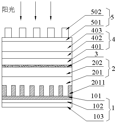
[0022] see figure 1 , the crystalline silicon / amorphous silicon thin-film laminated solar cell of the present invention is composed of a collector electrode layer 1, a bottom cell 2, a top cell 4, and a positive electrode layer 5 in sequence, and a layer is arranged between the bottom cell 2 and the top cell 4 Coupling film connection layer 3. The bottom cell 2 is a PN crystalline silicon cell prepared by forming a P-type diffusion layer 202 on an N-type crystalline silicon substrate 201 by a diffusion process. On the light-facing surface of the P-type diffusion layer 202 of the bottom cell 2, deposit a coupling thin-film connection layer 3 with a thickness of 0.1-100 nm, and the material is selected from one of ITO, ZnO, Ag, Cu, and Al. The top cell 4 is a PIN-type amorphous silicon thin film prepared by sequentially depositing an N-type amorphous silicon layer 401, an intrinsic amorphous silicon layer 402, and a P-type amorphous silicon layer 403 on the coupling layer 3 by ...

Embodiment 2

[0025] see still figure 1 , the crystalline silicon / amorphous silicon thin-film laminated solar cell of the present invention is composed of a collector electrode layer 1, a bottom cell 2, a top cell 4, and a positive electrode layer 5 in sequence, and a layer is arranged between the bottom cell 2 and the top cell 4 Coupling film connection layer 3. The bottom cell 2 is an NP crystalline silicon cell prepared by forming an N-type diffusion layer 202 on a P-type crystalline silicon substrate 201 by a diffusion process. On the N-type diffused layer 202 of the bottom cell 2 deposit a coupling thin-film connecting layer 3 with a thickness of 0.1-100 nm, and the material is selected from one of ITO, ZnO, Ag, Cu, and Al. The top cell 4 is a NIP-type amorphous silicon thin film prepared by sequentially depositing a P-type amorphous silicon layer 401, an intrinsic amorphous silicon layer 402, and an N-type amorphous silicon layer 403 on the coupling layer 3 by PECVD. Battery.

[00...


PUM


Abstract

The invention discloses a crystal silicon / amorphous silicon thin-film stacked solar cell, which is formed by sequentially stacking a collecting electrode layer, a bottom cell, a top cell and a positive electrode layer, wherein the bottom cell is a crystal silicon cell; the top cell is an amorphous silicon thin-film cell; a coupling thin film connection layer is arranged between the bottom cell and the top cell; a good conductor layer, a transparent semiconductor thin-film and a metal film are sequentially deposited on a backlight surface of the bottom cell to form the collecting electrode layer; and an ITO thin-film and a good conductor grating are sequentially deposited on a light-facing surface of the top cell to form the positive electrode layer. According to the crystal silicon / amorphous silicon thin-film stacked solar cell, a nanoscale good conductor thin-film is adopted between a crystal silicon cell and an amorphous silicon thin-film cell as a coupling connection structure; a good effect of coupling amplification of short-circuit current density JSC of a single-junction cell of the cell is put into a play when high superimposing open voltage and a relatively high filling factor are kept; and the defects of amorphous silicon and the influence on cell performance caused by crystal silicon and amorphous silicon interface quality are improved.

Description

technical field [0001] The invention relates to the technical field of solar cells, in particular to a crystalline silicon / amorphous silicon thin film laminated solar cell. Background technique [0002] The production technology of crystalline silicon solar cells is mature, the conversion efficiency is high and stable, and it is the leading product of solar cells at present. Although the development of solar cells needs to consider many factors such as cost, stability, and conversion efficiency, the improvement of conversion efficiency is still the most important consideration for solar cells. Due to the impact of the structure of the battery itself and the production process on light absorption, there is still a big gap between the conversion efficiency of batteries on the market and the efficiency records of laboratory solar cells. [0003] In the process of considering how to reduce silicon consumption and production costs, amorphous silicon thin film solar cells have be...

Claims


Application Information

Patent Timeline
Patent Type & Authority Applications(China)
IPC IPC(8): H01L31/078H01L31/0224
CPCY02E10/50
Inventor 宋太伟高伟波方祥杨光余文凤张长华
Owner SHANGHAI JIANYE TECH ENG
Why Eureka
Try Eureka