Wavelength conversion device, preparation method thereof and light-emitting device

A wavelength conversion device and excitation light technology, applied in the optical field, can solve the problems of high cost, low reflectivity, poor adhesion of metal reflective layers, etc.

Pending Publication Date: 2020-07-07
APPOTRONICS CORP LTD
View PDF5 Cites 1 Cited by
  • Summary
  • Abstract
  • Description
  • Claims
  • Application Information

AI Technical Summary

Problems solved by technology

However, the above technical methods require expensive high-purity targets and equipment, and have high requirements for the cleanliness and roughness of the ceramic surface
[0007] In summary, in the existing wavelength conversion device packaging technology, the technology of directly polishing the surface of the fluorescent ceramic layer and then coating the metal reflective layer has the problems of poor adhesion of the metal reflective layer and low reflectivity at the interface between the fluorescent ceramic layer and the metal reflective layer. ; and using techniques such as magnetron sputtering, vacuum evaporation, chemical vapor deposition or physical vapor deposition, the method of prefabricating a transition layer at the interface between the fluorescent ceramic layer and the metal reflective layer requires expensive high-purity targets and equipment, high cost

Method used


Image

  • Wavelength conversion device, preparation method thereof and light-emitting device
  • Wavelength conversion device, preparation method thereof and light-emitting device
  • Wavelength conversion device, preparation method thereof and light-emitting device

Examples


Embodiment Construction

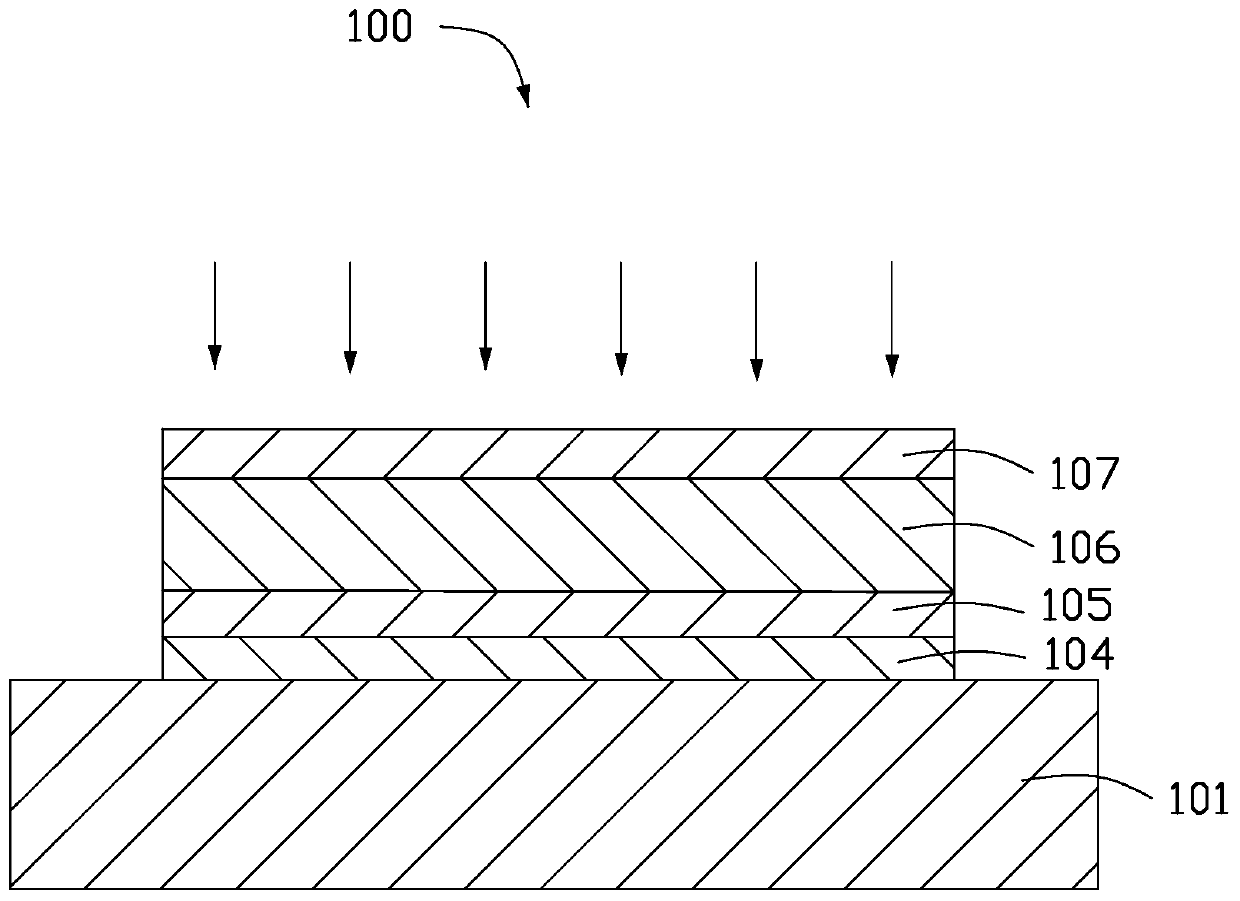
[0026] see figure 1 The wavelength conversion device 100 provided by an embodiment of the present invention at least includes a substrate 101, a metal reflective layer 104, a nano-silicon dioxide low-refractive index layer 105, a fluorescent ceramic layer 106, and a nano-silicon dioxide anti-reflection layer 107 that are sequentially stacked. . The nano-silica low-refractive index layer 105 and the nano-silica antireflection layer 107 are prepared by a sol-gel method.

[0027] In this embodiment, the excitation light generated by the light source irradiates the wavelength conversion device 100 from the side of the nano-silica anti-reflection layer 107 away from the substrate 101, and the fluorescent ceramic layer 106 converts the excitation light into a received light and emits it from the substrate 101. .

[0028] The nano-silica low-refractive index layer 105 and the nano-silica anti-reflection layer 107 are basically composed of nano-silica particles. The term "nano-sili...


PUM

PropertyMeasurementUnit
sizeaaaaaaaaaa
thicknessaaaaaaaaaa
thicknessaaaaaaaaaa

Abstract

The invention discloses a wavelength conversion device. The wavelength conversion device comprises a substrate, a metal reflecting layer, a nano silicon dioxide low-refractive-index layer, a fluorescent ceramic layer and a nano silicon dioxide anti-reflection layer which are sequentially stacked. The invention further provides a preparation method of the wavelength conversion device and a light-emitting device applying the wavelength conversion device. The preparation method comprises the steps of providing a fluorescent ceramic layer; forming a nano silicon dioxide low-refractive-index layerand a nano silicon dioxide anti-reflection layer on two opposite surfaces of the fluorescent ceramic layer by adopting a sol-gel method; forming a metal reflecting layer on the surface, which is awayfrom the fluorescent ceramic layer, of the nano silicon dioxide low-refractive-index layer; and providing a substrate, wherein the substrate, the metal reflecting layer, the nano silicon dioxide low-refractive-index layer, the fluorescent ceramic layer and the nano silicon dioxide anti-reflection layer are sequentially stacked.

Description

technical field [0001] The invention relates to the field of optical technology, in particular to a wavelength conversion device, a preparation method thereof, and a light emitting device using the wavelength conversion device. Background technique [0002] In the prior art, the main difficulties faced in the packaging technology of fixed wavelength conversion devices are: [0003] 1) The metal reflective layer set on the back of the fluorescent ceramic layer needs to take into account high reflectivity and thinner thickness. The usual practice is to directly polish the surface of the fluorescent ceramic layer and then coat the metal reflective layer. However, due to the difference in physical properties of the two materials , there will be problems that the metal reflective layer is easy to fall off and the adhesion is poor; and because the refractive index of the fluorescent ceramic layer is relatively high, the reflectivity at the interface of the metal reflective layer i...

Claims


Application Information

Patent Timeline
Patent Type & Authority Applications(China)
IPC IPC(8): G03B21/20F21V9/30
CPCF21V9/30G03B21/204F21V13/02G03B21/20
Inventor 陈雨叁段银祥刘莹莹李乾李屹
Owner APPOTRONICS CORP LTD
Why Eureka
Try Eureka