Area array sensor device and method of forming the same

A sensor device and sensor circuit technology, applied in the field of sensors, can solve the problems of poor reliability and large occupied area of ​​area array sensors, and achieve the effect of improving reliability and reducing occupied area.

Active Publication Date: 2018-08-21
SHANGHAI OXI TECH
View PDF6 Cites 0 Cited by
  • Summary
  • Abstract
  • Description
  • Claims
  • Application Information

AI Technical Summary

Problems solved by technology

[0007] The problem solved by the invention is that the reliability of the existing area array sensor is relatively poor, and the occupied area is relatively large

Method used


Image

  • Area array sensor device and method of forming the same
  • Area array sensor device and method of forming the same
  • Area array sensor device and method of forming the same

Examples


Embodiment Construction

[0041] In order to make the above objects, features and advantages of the present invention more comprehensible, specific embodiments of the present invention will be described in detail below in conjunction with the accompanying drawings.

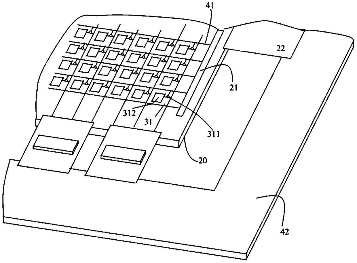
[0042] Such as image 3 As shown, the embodiment of the present invention provides an area sensor device, including: a driving circuit 21 and a sensor circuit, and the sensor circuit includes a pixel unit array composed of pixel units 31 and a driving line 41 connecting the pixel units. The pixel unit 31 includes: a second transistor 311 and a photoelectric device 312 , and the second transistor 311 is connected to the driving line 41 as a switching device. The pixel driving circuit 21 is adapted to turn on the pixel unit array row by row.

[0043] Such as Figure 4 As shown, this embodiment provides an implementation manner of the driving circuit 21 , and the driving circuit 21 includes m basic shift units 212 . The output terminal G1 ...


PUM


Abstract

An area array sensor device and its forming method, the area array sensor device includes: a drive circuit and a sensor circuit, the drive circuit and the sensor circuit are formed on the same substrate surface, and the sensor circuit includes a pixel unit array composed of pixel units and the driving line connected to the pixel unit, the output terminal of the driving circuit is connected to the driving line of the sensor circuit, the driving circuit includes a first transistor, and the pixel unit includes a second transistor; the first transistor includes The first shielding layer, the second transistor includes a second shielding layer. In the area array sensor device of the technical solution of the present invention, the components of the drive circuit and the sensor circuit can be manufactured on the same substrate, which reduces the occupied area and improves the reliability, and the formation process can be carried out synchronously without adding additional process steps.

Description

technical field [0001] The invention relates to the field of sensors, in particular to an area array fingerprint sensor device and a forming method thereof. Background technique [0002] The area sensor is a large-area planar imaging device, which is composed of a pixel unit array, driving lines, signal readout lines, etc. The optical signal with image information is directly projected to each pixel unit on the imaging surface of the sensor, and is absorbed by the pixel unit of the sensor to form an image. Since the light is focused without lenses or optical fibers, it is the same size and non-scaling imaging, so it will have better imaging quality; at the same time, the imaging equipment is lighter and thinner, so it has been widely used in various fields. [0003] For example, area array sensors used in fingerprint imaging, document scanning and other fields. Such as figure 1 As shown, the visible light penetrating from the back is irradiated to the object 13 that is cl...

Claims


Application Information

Patent Timeline
Patent Type & Authority Patents(China)
IPC IPC(8): H01L27/146H01L21/77
CPCH01L27/14678H01L27/14692G06V40/1329G06V40/1306H01L31/032H01L31/02164H01L31/028H01L31/03762H01L31/03682
Inventor 林崴平
Owner SHANGHAI OXI TECH
Why Eureka
Try Eureka