Circuit forming method of outer layer of circuit board
A technology for outer layer circuits and circuit boards, which is applied in chemical/electrolytic methods to remove conductive materials, inks, household appliances, etc. It can solve problems such as production costs that cannot be reduced, material waste, and dry films that cannot be broken through. Strong sealing ability, good scratch resistance and high hardness
Active Publication Date: 2016-02-17
深圳市乐建感光材料科技有限公司
View PDF4 Cites 5 Cited by
- Summary
- Abstract
- Description
- Claims
- Application Information
AI Technical Summary
Problems solved by technology
[0005] The use of dry film has been used in the circuit board process for more than 30 years. Although the dry film is better than the liquid wet film in terms of use and precision, however, since the dry film must be fused with photosensitive coating and PVC film, The production cost has been unable to decrease, and the development of dry film has not been able to break through in the last ten years. As mentioned above, the price has reached the limit of the cost, and there are also inevitable waste of materials in different degrees during application (such as There is excess dry film on the four sides of the board), therefore, in order to reduce waste and reduce the impact on the overall environment (disposal of the PVC sheet that protects the dry film also leads to environmental problems) and cost savings, the introduction and use of a new type of deep curing UV Photosensitive ink replaces dry film technology is a very valuable solution
Method used
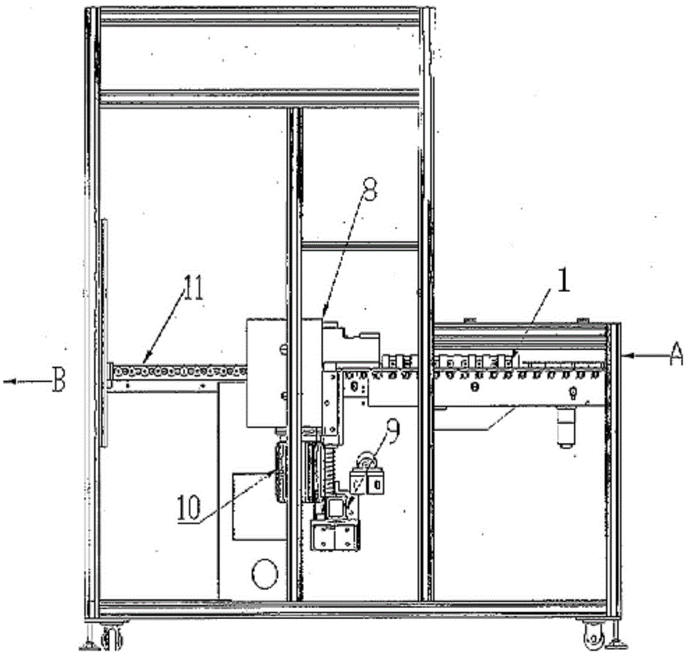
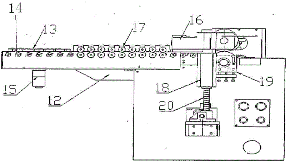
View moreImage
Smart ImageViewing Examples
Examples
Embodiment 1~4
[0074] According to the examples 1 to 4 in Table 2, the components of the deep layer UV curable ink are mixed with the solvent, and ground and mixed evenly at a temperature lower than 60°C to obtain the corresponding deep layer UV curable ink. Wherein, each component material is commercially available, and the molecular weight of the thermoplastic acrylic resin is about 10,000.
Login to View More PUM
| Property | Measurement | Unit |
|---|---|---|
| particle diameter | aaaaa | aaaaa |
| hardness | aaaaa | aaaaa |
Abstract
The invention relates to a circuit forming method of an outer layer of a circuit board. The method comprises: a circuit board with an outer layer circuit needing to be processed is provided; pouring and coating of deep-curing UV ink are carried out on a hole needing protection and / or a predetermined region needing protection at a circuit board surface on the circuit board; exposure is carried out on the condition of 100-300mJ / cm<2>; and development, etching, and membrane removing are carried out on the exposed circuit board to form an outer layer circuit of the circuit board. According to the invention, the deep-curing UV ink is used for manufacturing the circuit board and the inside of the hole and the region with the surface needing protection are coated with the ink; and deep curing can be realized after UV light source irradiation. Therefore, chemical impacts on a weak base developing solution with the pH being approximately equal to 10 and an acid etching solution with the pH being 2 to 3 and thus the anti-etching effect is realized.
Description
technical field [0001] The invention relates to a method for forming the outer circuit of a circuit board. Specifically, the invention relates to a method for using deep-cured UV ink instead of a dry film as a temporary protective film layer in the forming process of the outer circuit of a circuit board. Background technique [0002] Circuit boards are regarded as an indispensable and important part in the rapidly developing electronics industry. The continuous improvement of circuits is to make continuous breakthroughs in the function and volume of electronic products. With the popularization of electronic products such as mobile phones and the ever-increasing functional requirements, the precision and complexity of circuit boards are also increasing day by day. All types of electronic products require circuit boards of varying complexity. [0003] In the prior art, two processes are usually used to manufacture the outer layer circuit of the circuit board. The first proce...
Claims
Login to View More Application Information
Patent Timeline
 Patent Type & Authority Applications(China)
IPC IPC(8): H05K3/06C09D11/101C09D11/107C09D11/102C09D11/03
CPCC09D11/03C09D11/101C09D11/102C09D11/107H05K3/06
Inventor 柯明喜
Owner 深圳市乐建感光材料科技有限公司


