Method for manufacturing printed circuit board and printed circuit board

A technology of printed circuit board and manufacturing method, which is applied in the direction of printed circuit manufacturing, printed circuit, and the formation of electrical connection of printed components, etc., which can solve the problem of insufficient adhesion between a conductive paste layer and a substrate, increased interface separation or detachment, failure to Solve problems such as practical use, and achieve the effects of preventing leakage, shortening the process, and preventing damage

Active Publication Date: 2016-03-02
INKTEC CO LTD
View PDF6 Cites 6 Cited by
  • Summary
  • Abstract
  • Description
  • Claims
  • Application Information

AI Technical Summary

Problems solved by technology

[0012] However, the method requires forming a printed circuit from a conductive paste by a printing method and filling the through hole with the conductive paste, but the printing method of forming the conductive part of the printed circuit from the conductive paste filling the through hole to form a protrusion is extremely limited. The conductive paste that is easy to form the conductive part of the printed circuit is difficult to fill the through hole and form a protrusion
In addition, the flexible printed circuit board manufactured in this way has the disadvantage that the connection part formed in the through hole will shrink or break under thermal or physical impact, and the possibility of disconnection is high, and there is also a need for further steps in the process. The disadvantage of adding a process that forms an additional closing plate part for preventing the leakage of the conductive paste filled in the through hole, so it has not been applied in the industry so far
In addition, since the adhesive force between the conductive paste layer and the base material is not sufficient, separation or detachment of the interface between the printed circuit formed by the conductive paste and the connecting conductor part forming the via hole protrusion increases, so it has not been practically used. change

Method used


Image

  • Method for manufacturing printed circuit board and printed circuit board
  • Method for manufacturing printed circuit board and printed circuit board
  • Method for manufacturing printed circuit board and printed circuit board

Examples


no. 1 example

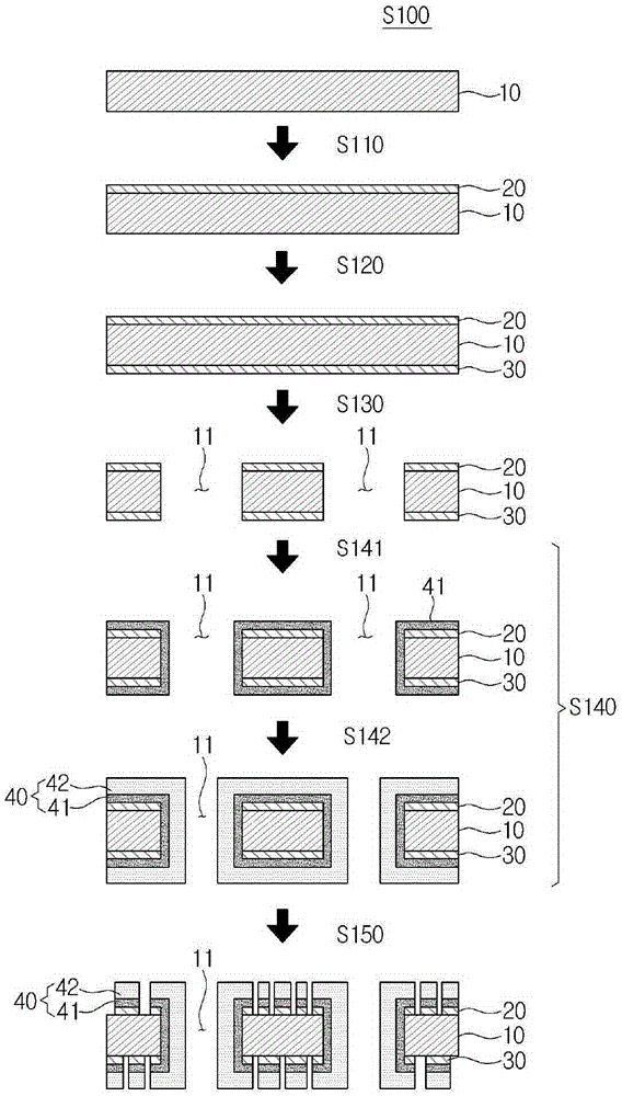
[0063] figure 1 It is a figure which schematically shows the process flow of the manufacturing method of the printed circuit board of 1st Example of this invention.

[0064] like figure 1 As shown, the manufacturing method S100 of the printed circuit board according to the first embodiment of the present invention includes the forming step S110 of the first coating, the forming step S120 of the second coating, the perforating step S130, the plating step S140 and the formation of the circuit pattern Step S150.

[0065] The step S110 of forming the first coating layer and the step S120 of forming the second coating layer are the steps of coating the first coating layer 20 and the second coating layer 30 on the upper surface and the lower surface of the substrate 10 respectively. In addition, although a polyimide film (PI: PolyImideFilm) was used as the substrate 10 in this step, it is not limited thereto.

[0066] The conductive ink is coated on the prepared upper surface of ...

no. 2 example

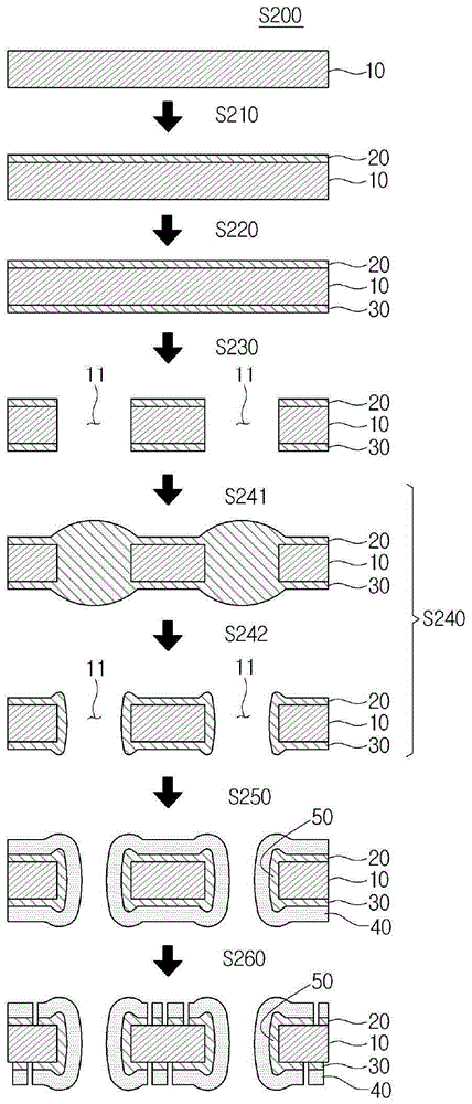
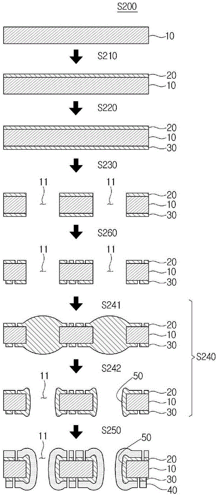
[0080] figure 2 It is a figure which schematically shows the process flow of the manufacturing method of the printed wiring board which concerns on the 2nd Embodiment of this invention.

[0081] like figure 2 As shown, the manufacturing method S200 of the printed circuit board according to the second embodiment of the present invention includes the forming step S210 of the first coating layer, the forming step S220 of the second coating layer, the perforating step S230, the forming step S240 of the conductive layer, and the plating step. Step S250 and step S260 of forming a circuit pattern.

[0082] The step S210 of forming the first coating and the step S220 of forming the second coating are the steps of coating the first coating 20 and the second coating 30 on the upper surface and the lower surface of the substrate 10 respectively. In addition, a polyimide film (PI: PolyImideFilm) may be used as the substrate 10 in this step, but is not limited thereto.

[0083] The co...

no. 3 example

[0100] Figure 4 It is a figure which schematically shows the process flow of the manufacturing method of the printed circuit board of the 3rd Embodiment of this invention.

[0101] like Figure 4 As shown, the manufacturing method S300 of the printed circuit board according to the third embodiment of the present invention includes the forming step S310 of the first coating layer, the forming step S320 of the second coating layer, the perforating step S330, the bonding step S340 of the temporary sealing layer, The forming step S350 of the conductive layer, the removing step S360 of the temporary plugging layer, the plating step S370 and the forming step S380 of the circuit pattern.

[0102] The step S310 of forming the first coating and the step S320 of forming the second coating are the steps of coating the first coating 20 and the second coating 30 on the upper surface and the lower surface of the substrate 10 respectively. In addition, a polyimide film (PI: PolyImideFilm)...


PUM


Abstract

The invention relates to a method for manufacturing a printed circuit board. The method for manufacturing the printed circuit board of the present invention comprises: a first coating layer formation step for forming a first coating layer on one surface of a substrate using conductive ink; a second coating layer formation step for forming a second coating layer on the other surface of the substrate using the conductive ink; a punching step for forming a through-hole by punching the first coating layer, the substrate, and the second coating layer; and a plating step for forming a plating layer by plating the first coating layer, the second coating layer, and an inner wall surface of the through-hole. Accordingly, the present invention provides the method for manufacturing the printed circuit board and the printed circuit board, which: can improve circuit pattern implementation accuracy and electrical properties through a conventional photography process when compared to the limitation of circuit pattern implementation and electric properties in a circuit fabrication process due to the existing printing method; can save base materials; can shorten a manufacturing process; and can improve productivity.

Description

technical field [0001] The present invention relates to a method for manufacturing a printed circuit board and a printed circuit board, and more specifically relates to a printed circuit board capable of forming a circuit pattern with fine and excellent conductive properties, saving raw materials and shortening the process, etc. Manufacturing method and printed circuit board. Background technique [0002] Generally speaking, a printed circuit board (Printed Circuit Board) is an electronic component in the form of a substrate on which various electronic components are loaded and electrically connected. [0003] According to the hard and soft materials of the substrate, printed circuit boards are divided into two categories: rigid printed circuit boards (Rigid Printed Circuit Board) and flexible printed circuit boards (Flexible Circuit Board). Recently, hard and soft composite printed circuit boards have appeared. [0004] In the initial stage of the application of printed ci...

Claims


Application Information

Patent Timeline
Patent Type & Authority Applications(China)
IPC IPC(8): H05K3/42
CPCH05K3/4069H05K3/12H05K3/246H05K3/427
Inventor 郑光春尹光伯韩英求尹东国金修汉
Owner INKTEC CO LTD
Why Eureka
Try Eureka