Thin film transistor, manufacturing method thereof, array substrate, and display device

A thin film transistor and array substrate technology, applied in the display field, can solve the problems of large leakage current, short display time and high refresh frequency

Active Publication Date: 2016-03-09
BOE TECH GRP CO LTD
View PDF4 Cites 29 Cited by
  • Summary
  • Abstract
  • Description
  • Claims
  • Application Information

AI Technical Summary

Problems solved by technology

[0004] Although the carrier mobility of the low-temperature polysilicon thin film transistor is relatively high, its leakage current in the off state is large, which causes the display device to maintain a frame display for a short time, resulting in the display device must be driven by high frequency (ie The refresh rate of the screen is high), and the high-frequency drive will undoubtedly increase the power consumption of the display device

Method used


Image

  • Thin film transistor, manufacturing method thereof, array substrate, and display device
  • Thin film transistor, manufacturing method thereof, array substrate, and display device
  • Thin film transistor, manufacturing method thereof, array substrate, and display device

Examples


Embodiment 1

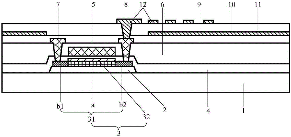
[0037] see figure 1 , this embodiment provides a thin film transistor, the thin film transistor includes a semiconductor layer 3, the semiconductor layer 3 includes a first semiconductor layer 31 and a second semiconductor layer 32, the first semiconductor layer 31 and the second semiconductor layer 32 are stacked, The material of the first semiconductor layer 31 is low temperature polysilicon, and the carrier mobility of the second semiconductor layer 32 is lower than that of the first semiconductor layer 31 .

[0038] The semiconductor layer of the low-temperature polysilicon thin film transistor in the prior art is only formed of low-temperature polysilicon, which causes electrons to pass through the low-temperature polysilicon regardless of whether the thin film transistor is in an on state or an off state. High, thus resulting in high carrier mobility and high concentration of the current in the off state, that is, a large leakage current. Compared with the prior art, th...

Embodiment 2

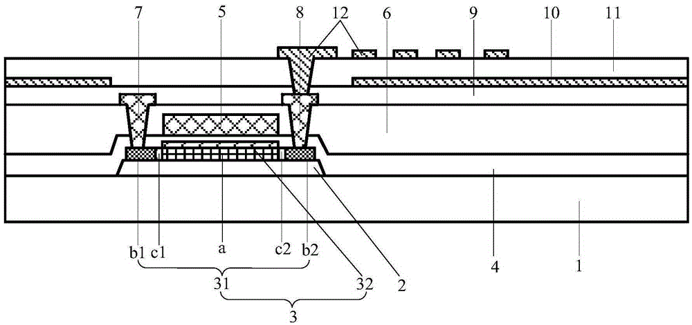
[0046] Based on Example 1, such as figure 2 As shown, in the thin film transistor provided in this embodiment, the first lightly doped region c1 is set between the first heavily doped region b1 and the channel region a of the first semiconductor layer 31, and the second heavily doped A second lightly doped region c2 is provided between the region b2 and the channel region a.

[0047] Since the concentration of metal ions doped in the lightly doped region is less than the concentration of metal ions doped in the heavily doped region, the resistance of the lightly doped region is smaller than that of the heavily doped region, so that in the first semiconductor On the premise that the size of the layer 31 remains unchanged, it is equivalent to increasing the resistance of the first semiconductor layer 31, that is, increasing the resistance on the electron conduction path, and further reducing the leakage current of the thin film transistor in the off state.

Embodiment 3

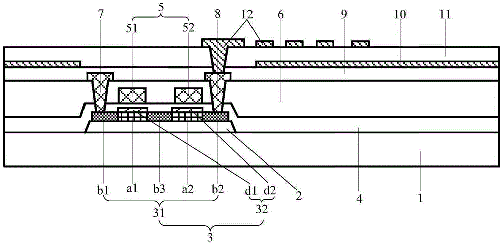
[0049] Based on Example 1, such as image 3 As shown, in the thin film transistor provided in this embodiment, the channel region a of the first semiconductor layer 31 includes a first channel region a1 and a second channel region a2; the first semiconductor layer 31 also includes a third heavily doped region b3, the third heavily doped region b3 is located between the first channel region a1 and the second channel region a2. The second semiconductor layer 32 includes a third channel region d1 and a fourth channel region d2, the orthographic projection of the third channel region d1 on the first channel region a1 is located in the first channel region a1, the first channel region a1 Orthographic projections of the four channel regions d2 on the second channel region a2 are located in the second channel region a2. The gate 5 in the thin film transistor includes a first gate 51 and a second gate 52, the first gate 51 is set corresponding to the first channel region a1, and the ...


PUM


Abstract

The present invention provides a manufacturing method of a thin film transistor, an array substrate and a display device, relating to the technical field of display. The invention is used for solving the problems of large current, high power consumption of a low-temperature polysilicon thin film transistor. The thin film transistor comprises semiconductor layers comprising a first semiconductor layer and a second semiconductor layer, and the first semiconductor layer and the second semiconductor layer are laminated. The material of the first semiconductor layer is low-temperature polysilicon, and the carrier mobility of the second semiconductor layer is smaller than the carrier mobility of the first semiconductor layer. The above thin film transistor is used in the array substrate, and pixels are driven.

Description

technical field [0001] The present invention relates to the field of display technology, in particular to a thin film transistor, a manufacturing method thereof, an array substrate, and a display device. Background technique [0002] A thin film transistor (Thin Film Transistor, TFT for short) is a key device of a display device, and each pixel in the display device is driven by a thin film transistor integrated in the pixel. [0003] Thin-film transistors generally include a gate, a semiconductor layer, a source, and a drain. According to different semiconductor layer materials, thin-film transistors can be divided into amorphous silicon (a-Si: H), low-temperature polysilicon (LowTemperaturePoly-Silicon, LTPS for short), There are various types of high temperature polysilicon (HTPS for short), oxide semiconductors, etc. Among them, low temperature polysilicon thin film transistors are widely used due to their advantages of high carrier mobility. [0004] Although the carri...

Claims


Application Information

Patent Timeline
Patent Type & Authority Applications(China)
IPC IPC(8): H01L29/786H01L29/24H01L29/423H01L21/336
CPCH01L29/24H01L29/42384H01L29/66757H01L29/78675H01L29/7869H01L29/78696
Inventor 李正亮曹占锋关峰姚琪张斌高锦成何晓龙孙雪菲
Owner BOE TECH GRP CO LTD
Why Eureka
Try Eureka